MPC5604B/C Microcontroller Reference Manual, Rev. 8
666 Freescale Semiconductor
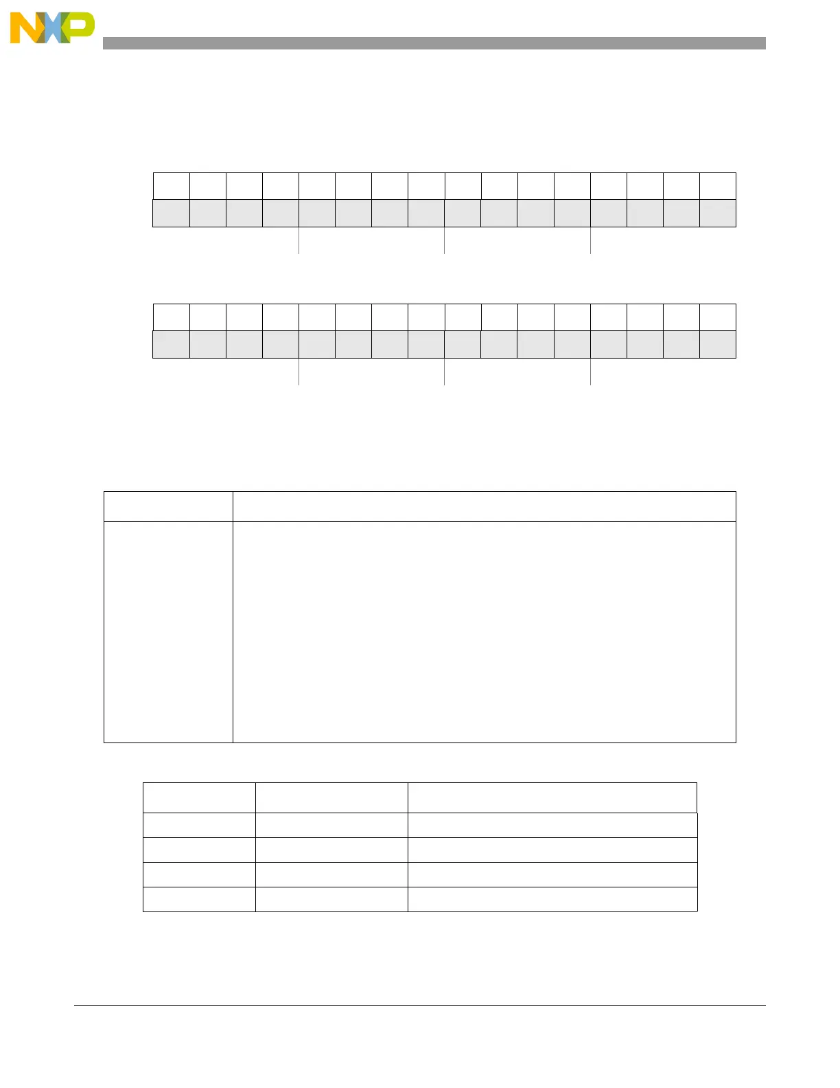
27.5.1.5 CFlash Address Register (CFLASH_ADR)
The CFLASH_ADR provides the first failing address in the event module failures (ECC or FPEC) occur
or the first address at which an ECC single error correction occurs.
Offset: 0x00018 Access: Read
0 1 2 3 4 5 6 7 8 9 10 11 12 13 14 15
R
0 0 0 0 0 0 0 0 0 AD22 AD21 AD20 AD19 AD18 AD17 AD16
W
Reset
0000000000000000
16 17 18 19 20 21 22 23 24 25 26 27 28 29 30 31
R
AD15 AD14 AD13 AD12 AD11 AD10 AD9 AD8 AD7 AD6 AD5 AD4 AD3 0 0 0
W
Reset
0000000000000000
Figure 27-9. CFlash Address Register (CFLASH_ADR)
Table 27-19. CFLASH_ADR field descriptions
Field Description
AD ADdress 22-3 (Read Only)
The Address Register provides the first failing address in the event of ECC error
(CFLASH_MCR[EER] = 1) or the first failing address in the event of RWW error
(CFLASH_MCR[RWE] = 1), or the address of a failure that may have occurred in a FPEC
operation (CFLASH_MCR[PEG] = 0). The Address Register also provides the first address
at which an ECC single error correction occurs (CFLASH_MCR[EDC] = 1).
The ECC double error detection takes the highest priority, followed by the FPEC error and
the ECC single error correction. When accessed CFLASH_ADR will provide the address
related to the first event occurred with the highest priority. The priorities between these four
possible events is summarized in Table 27-20.
This address is always a Double Word address that selects 64 bits.
In case of a simultaneous ECC Double Error Detection on both Double Words of the same
page, bit AD3 will output 0. The same is valid for a simultaneous ECC Single Error Correction
on both Double Words of the same page.
Table 27-20. CFLASH_ADR content: priority list
Priority level Error flag CFLASH_ADR content
1 CFLASH_MCR[EER] = 1 Address of first ECC Double Error
2 CFLASH_MCR[RWE] = 1 Address of first RWW Error
3 CFLASH_MCR[PEG] = 0 Address of first FPEC Error
4 CFLASH_MCR[EDC] = 1 Address of first ECC Single Error Correction