MPC5604B/C Microcontroller Reference Manual, Rev. 8
Freescale Semiconductor 667
27.5.1.6 CFlash User Test 0 register (CFLASH_UT0)
The User Test Registers provide the user with the ability to test features on the flash memory module. The
User Test 0 Register allows to control the way in which the flash memory content check is done.
Bits MRE, MRV, AIS, EIE and DSI[7:0] of the User Test 0 Register are not accessible whenever
CFLASH_MCR[DONE] or UT0[AID] are low: reading returns indeterminate data while writing has no
effect.
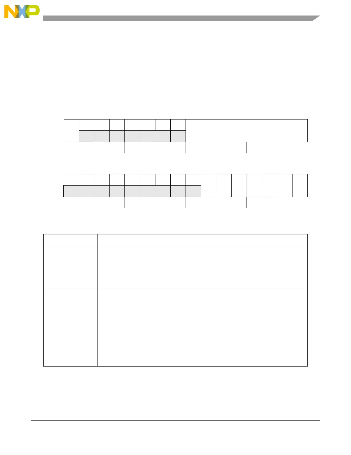
Offset: 0x0003C Access: Read/write
0123456789101112131415
R
UTE0000000
DSI
W
w1c
Reset
0000000000000000
16 17 18 19 20 21 22 23 24 25 26 27 28 29 30 31
R
000000000
X MRE MRV EIE AIS AIE AID
W
Reset
0000000000000001
Figure 27-10. CFlash User Test 0 register (CFLASH_UT0)
Table 27-21. CFLASH_UT0 field descriptions
Field Description
UTE User Test Enable
This status bit gives indication when User Test is enabled. All bits in CFLASH_UT0-2 and
CFLASH_UMISR0-4 are locked when this bit is 0.
The method to set this bit is to provide a password, and if the password matches, the UTE
bit is set to reflect the status of enabled, and is enabled until it is cleared by a register write.
For UTE the password 0xF9F99999 must be written to the CFLASH_UT0 register.
DSI Data Syndrome Input
These bits represent the input of Syndrome bits of ECC logic used in the ECC Logic Check.
Bits DSI[7:0] correspond to the 8 syndrome bits on a double word.
These bits are not accessible whenever CFLASH_MCR[DONE] or CFLASH_UT0[AID] are
low: reading returns indeterminate data while writing has no effect.
0: The syndrome bit is forced at 0.
1: The syndrome bit is forced at 1.
X Reserved
This bit can be written and its value can be read back, but there is no function associated.
This bit is not accessible whenever CFLASH_MCR[DONE] or CFLASH_UT0[AID] are low:
reading returns indeterminate data while writing has no effect.
 Loading...