MPC5604B/C Microcontroller Reference Manual, Rev. 8
Freescale Semiconductor 641
The high voltages needed for program/erase operations are generated internally.
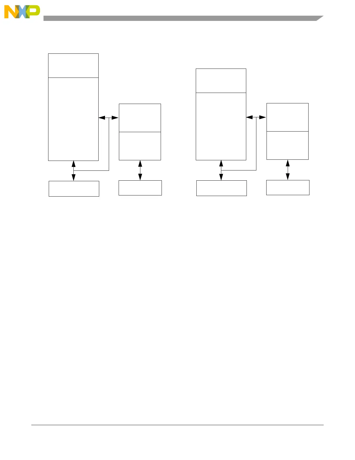
Figure 27-2. CFlash and DFlash module structures
27.4 Functional description
27.4.1 Module structure
The flash memory module is addressable by Double Word (64 bits) for program, and page (128 bits) for
read. Reads to the flash memory always return 128 bits, although read page buffering may be done in the
platform flash memory controller.
Each read of the flash memory module retrieves a page, or four consecutive words (128 bits) of
information. The address for each word retrieved within a page differs from the other addresses in the page
only by address bits (3:2).
The flash memory module supports fault tolerance through Error Correction Code (ECC) or error
detection, or both. The ECC implemented within the flash memory module will correct single bit failures
and detect double bit failures.
The flash memory module uses an embedded hardware algorithm implemented in the Memory Interface
to program and erase the flash memory core.
The embedded hardware algorithm includes control logic that works with software block enables and
software lock mechanisms to guard against accidental program/erase.
512 KB:
+ 16 KB TestFlash
HV generator
Flash memory
Controller
Flash memory
Matrix
Register
Program/Erase
registers
interface
Flash memory
interface
+ 16 KB Shadow
bank 0
CFlash structure
64 KB:
+ 16 KB TestFlash
HV generator
Flash memory
Controller
Flash memory
Matrix
Register
Program/Erase
registers
interface
Flash memory
interface
bank 1
DFlash structure
32 KB
2 × 16 KB
2 × 32 KB
3 × 128 KB
4 × 16 KB