MPC5604B/C Microcontroller Reference Manual, Rev. 8
Freescale Semiconductor 225
11.1.6 Register description
The VREG_CTL register is mapped to the MC_PCU address space as described in Chapter 10, Power
Control Unit (MC_PCU).
11.2 Power supply strategy
From a power-routing perspective, the device is organized as follows.
The device provides four dedicated supply domains at package level:
1. HV (high voltage external power supply for I/Os and most analog module) — This must be
provided externally through VDD_HV/VSS_HV power pins. Voltage values should be aligned
with V
DD
/V
SS
. Refer to data sheet for details.
2. ADC (high voltage external power supply for ADC module) — This must be provided externally
through VDD_HV_ADC/VSS_HV_ADC power pins. Voltage values should be aligned with
V
DD_HV_ADC
/V
SS_HV_ADC
. Refer to data sheet for details.
3. BV (high voltage external power supply for voltage regulator module) — This must be provided
externally through VDD_BV_/VSS_BV power pins. Voltage values should be aligned with
V
DD
/V
SS
. Refer to data sheet for details.
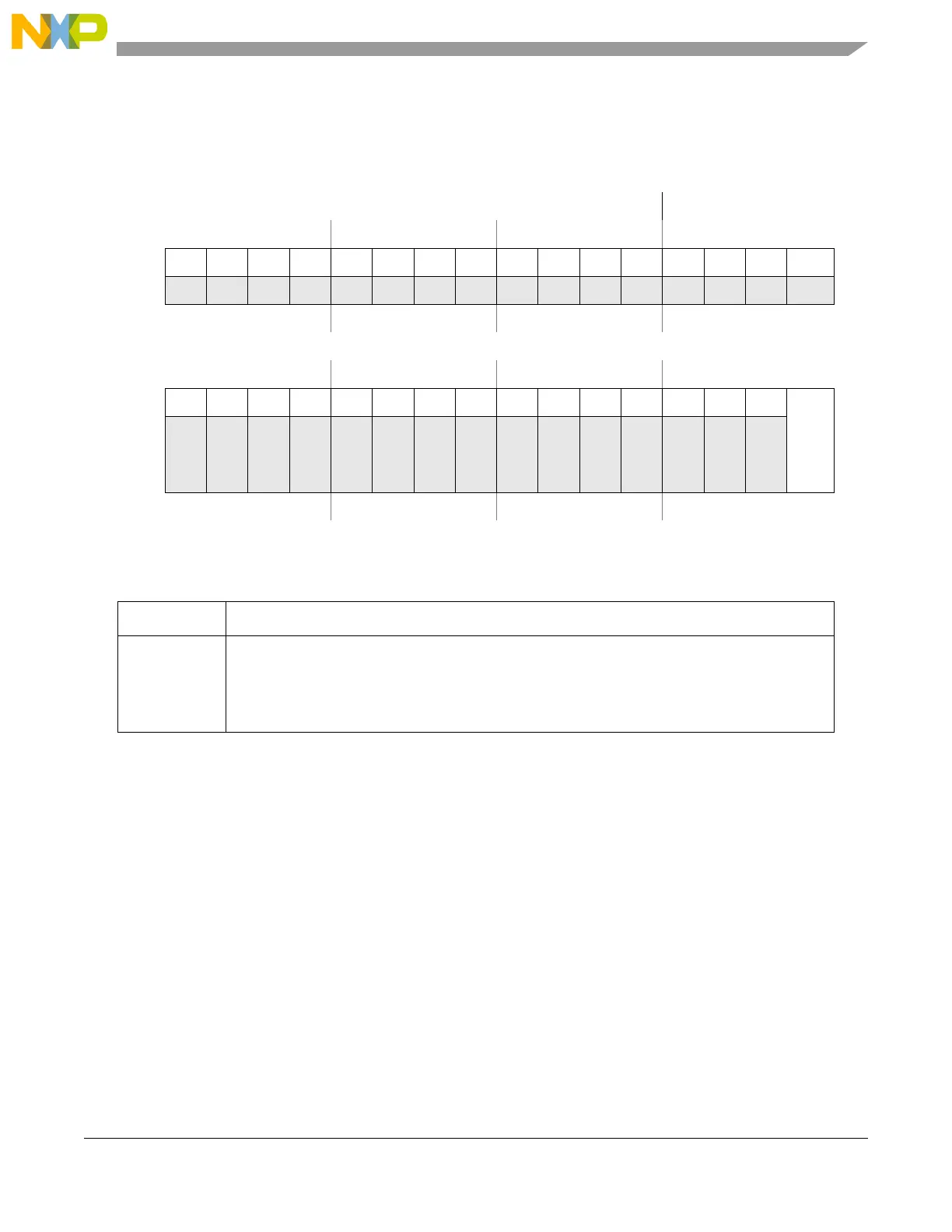
Address: 0xC3FE_8080 Access: User read/write
0123456789101112131415
R000000000000000 0
W
Reset000000000000000 0
16 17 18 19 20 21 22 23 24 25 26 27 28 29 30 31
R000000000000000
5V_LVD_MASK
W
Reset000000000000000 1
Figure 11-1. Voltage Regulator Control Register (VREG_CTL)
Table 11-1. VREG_CTL field descriptions
Field Description
5V_LVD_MASK Mask bit for 5 V LVD from regulator
This is a read/write bit and must be unmasked by writing a ‘1’ by software to generate LVD
functional reset request to MC_RGM for 5 V trip.
1: 5 V LVD is masked
0: 5 V LVD is not masked.