MPC5604B/C Microcontroller Reference Manual, Rev. 8
Freescale Semiconductor 131
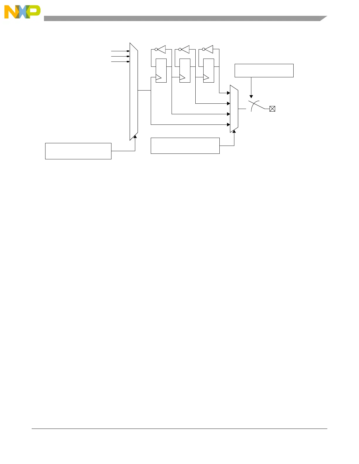
7.6.3 Output Clock Division Selection
The MC_CGM provides the following output signals for the output clock generation:
• PA[0] (see Figure 7-7). This signal is generated by utilizing one of the 3-stage ripple counter
outputs or the selected signal without division. The non-divided signal is not guaranteed to be 50%
duty cycle by the MC_CGM.
• the MC_CGM also has an output clock enable register (see Section 7.5.1.1, “Output Clock Enable
Register (CGM_OC_EN)) which contains the output clock enable/disable control bit.
CGM_OCDS_SC.SELCTL
CGM_OCDS_SC.SELDIV
0
1
2
3
Register
Register
Figure 7-7. MC_CGM Output Clock Multiplexer and PA[0] Generation
4-16 MHz ext. xtal osc. 0
16 MHz int. RC osc. 1
freq. mod. PLL 2
PA[0]
’0’
CGM_OC_EN Register