MPC5604B/C Microcontroller Reference Manual, Rev. 8
126 Freescale Semiconductor
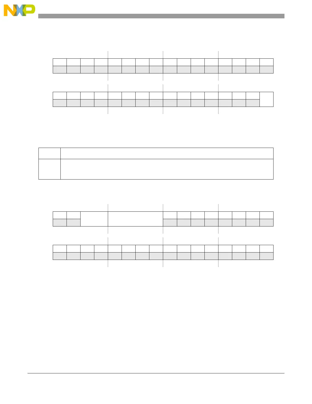
7.5.1.1 Output Clock Enable Register (CGM_OC_EN)
This register is used to enable and disable the output clock.
7.5.1.2 Output Clock Division Select Register (CGM_OCDS_SC)
This register is used to select the current output clock source and by which factor it is divided before being
delivered at the output clock.
Address 0xC3FE_0370 Access: Supervisor read/write
0123456789101112131415
R0000000000000000
W
Reset0000000000000000
16 17 18 19 20 21 22 23 24 25 26 27 28 29 30 31
R000000000000000
EN
W
Reset0000000000000000
Figure 7-2. Output Clock Enable Register (CGM_OC_EN)
Table 7-3. Output Clock Enable Register (CGM_OC_EN) Field Descriptions
Field Description
EN Output Clock Enable control
0 Output Clock is disabled
1 Output Clock is enabled
Address 0xC3FE_0374 Access: Supervisor read/write
0123456789101112131415
R0 0
SELDIV SELCTL
00000000
W
Reset0000000000000000
16 17 18 19 20 21 22 23 24 25 26 27 28 29 30 31
R0000000000000000
W
Reset0000000000000000
Figure 7-3. Output Clock Division Select Register (CGM_OCDS_SC)