MPC5604B/C Microcontroller Reference Manual, Rev. 8
502 Freescale Semiconductor
23.6.4.3 After SCK delay (t
ASC
)
The after SCK_x delay is the length of time between the last edge of SCK_x and the negation of CS_x. See
Figure 23-16 and Figure 23-17 for illustrations of the after SCK_x delay. The PASC and ASC fields in the
DSPIx_CTARn registers select the after SCK delay. The relationship between these variables is given in
the following formula:
Table 23-27 shows an example of the computed after SCK delay.
23.6.4.4 Delay after transfer (t
DT
)
The delay after transfer is the length of time between negation of the CSx signal for a frame and the
assertion of the CSx signal for the next frame. The PDT and DT fields in the DSPIx_CTARn registers
select the delay after transfer.
See Figure 23-16 for an illustration of the delay after transfer.
The following formula expresses the PDT/DT/delay after transfer relationship:
Table 23-28 shows an example of the computed delay after transfer.
23.6.4.5 Peripheral chip select strobe enable (CS5_x)
The CS5_x signal provides a delay to allow the CSx signals to settle after transitioning thereby avoiding
glitches. When the DSPI is in master mode and PCSSE bit is set in the DSPIx_MCR, CS5_x provides a
signal for an external demultiplexer to decode the CS4_x signals into as many as 32 glitch-free CSx
signals.
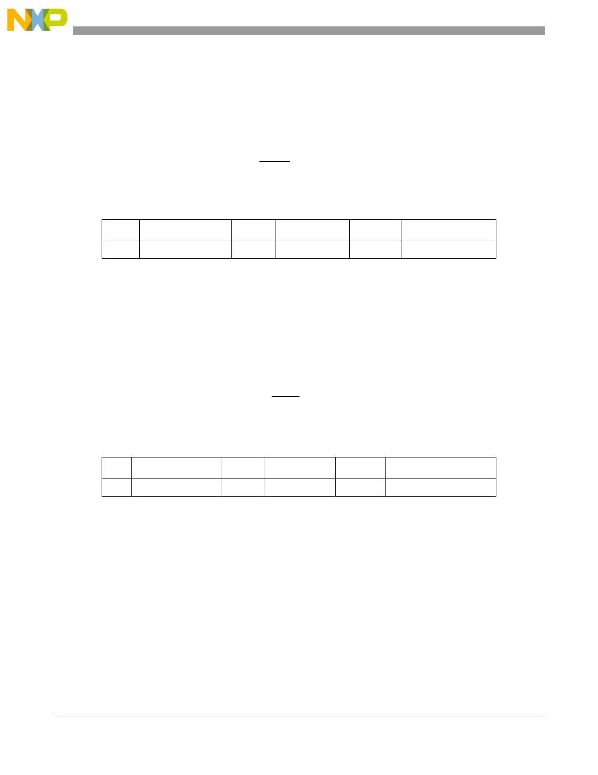
Table 23-27. After SCK delay computation example
PASC Prescaler value ASC Scaler value f
SYS
After SCK delay
0b01 3 0b0100 32 64 MHz 1.5 µs
Table 23-28. Delay after transfer computation example
PDT Prescaler value DT Scaler value f
SYS
Delay after transfer
0b01 3 0b1110 32768 64 MHz 1.54 ms