MPC5604B/C Microcontroller Reference Manual, Rev. 8
644 Freescale Semiconductor
Erase of the TestFlash block is always locked.
User mode program of the TestFlash block are enabled only when MCR[PEAS] is high.
The TestFlash block may be locked/unlocked against program by using the LML[TSLK] and
SLL[STSLK] registers.
Programming of the TestFlash block has similar restrictions as the array in terms of how ECC is calculated.
Only one programming operation is allowed per 64-bit ECC segment.
The first 8 KB of TestFlash block may be used for user defined functions (possibly to store serial numbers,
other configuration words or factory process codes). Locations of the TestFlash other than the first 8 KB
of OTP area cannot be programmed by the user application.
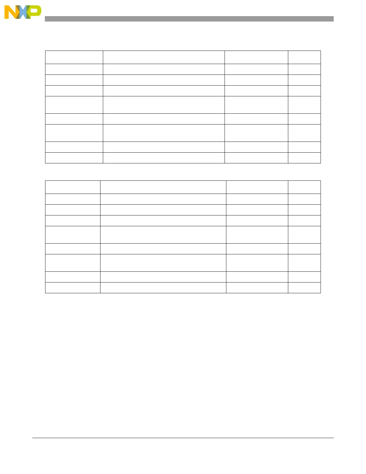
Table 27-4. CFlash TestFlash structure
Name Description Addresses Size
— User OTP area 0x400000–0x401FFF 8192 bytes
— Reserved 0x402000–0x403CFF 7424 bytes
— User OTP area 0x403D00–0x403DE7 232 bytes
CFLASH_NVLML CFlash Nonvolatile Low/Mid Address Space Block
Locking Register
0x403DE8–0x403DEF 8 bytes
— Reserved 0x403DF0–0x403DF7 8 bytes
CFLASH_NVSLL CFlash Nonvolatile Secondary Low/mid Address
Space Block Locking Register
0x403DF8–0x403DFF 8 bytes
— User OTP area 0x403E00–0x403EFF 256 bytes
— Reserved 0x403F00–0x403FFF 256 bytes
Table 27-5. DFlash TestFlash structure
Name Description Addresses Size
— User OTP area 0xC00000–0xC01FFF 8192 bytes
— Reserved 0xC02000–0xC03CFF 7424 bytes
— User OTP area 0xC03D00–0xC03DE7 232 bytes
DFLASH_NVLML DFlash Nonvolatile Low/Mid Address Space Block
Locking Register
0xC03DE8–0xC03DEF 8 bytes
— Reserved 0xC03DF0–0xC03DF7 8 bytes
DFLASH_NVSLL DFlash Nonvolatile Secondary Low/Mid Address
Space Block Locking Register
0xC03DF8–0xC03DFF 8 bytes
— User OTP area 0xC03E00–0xC03EFF 256 bytes
— Reserved 0xC03F00–0xC03FFF 256 bytes