MPC5604B/C Microcontroller Reference Manual, Rev. 8
Freescale Semiconductor 315
18.5.2.4.3 MPU Region Descriptor n, Word 2 (MPU_RGDn.Word2)
The third word of the MPU region descriptor defines the access control rights of the memory region. The
access control privileges are dependent on two broad classifications of bus masters. Bus masters 0–3 are
typically reserved for processor cores and the corresponding access control is a 6-bit field defining
separate privilege rights for user and supervisor mode accesses as well as the optional inclusion of a
process identification field within the definition. Bus masters 4–7 are typically reserved for data movement
engines and their capabilities are limited to separate read and write permissions. For these fields, the bus
master number refers to the logical master number defined as the XBAR hmaster[3:0] signal.
For the processor privilege rights, there are three flags associated with this function: {read, write, execute}.
In this context, these flags follow the traditional definition:
• Read (r) permission refers to the ability to access the referenced memory address using an operand
(data) fetch.
•Write (w) permission refers to the ability to update the referenced memory address using a store
(data) instruction.
• Execute (x) permission refers to the ability to read the referenced memory address using an
instruction fetch.
The evaluation logic defines the processor access type based on multiple AHB signals, as hwrite and
hprot[1:0].
For non-processor data movement engines (bus masters 4–7), the evaluation logic simply uses hwrite to
determine if the access is a read or write.
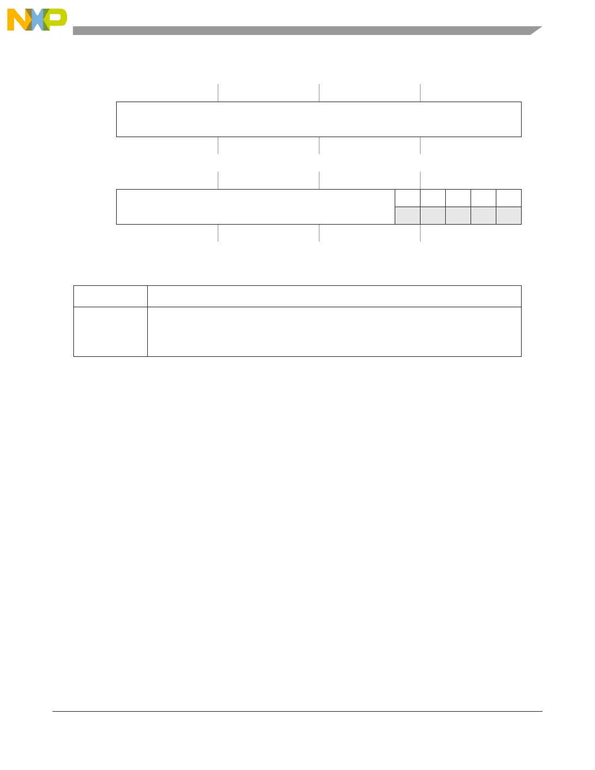
Offset: 0x400 + (16*n) + 0x4 (MPU_RGDn.Word1) Access: Read/write
0123456789101112131415
R
ENDADDR[26:11]
W
Reset––––––––––––––––
16 17 18 19 20 21 22 23 24 25 26 27 28 29 30 31
R
ENDADDR[10:0]
11111
W
Reset–––––––––––11111
Figure 18-6. MPU Region Descriptor, Word 1 Register (MPU_RGDn.Word1)
Table 18-6. MPU_RGDn.Word1 field descriptions
Field Description
ENDADDR End Address
This field defines the most significant bits of the 31-modulo-32 byte end address of the memory
region. There are no hardware checks to verify that ENDADDR >= SRTADDR; it is software’s
responsibility to properly load these region descriptor fields.