MPC5604B/C Microcontroller Reference Manual, Rev. 8
508 Freescale Semiconductor
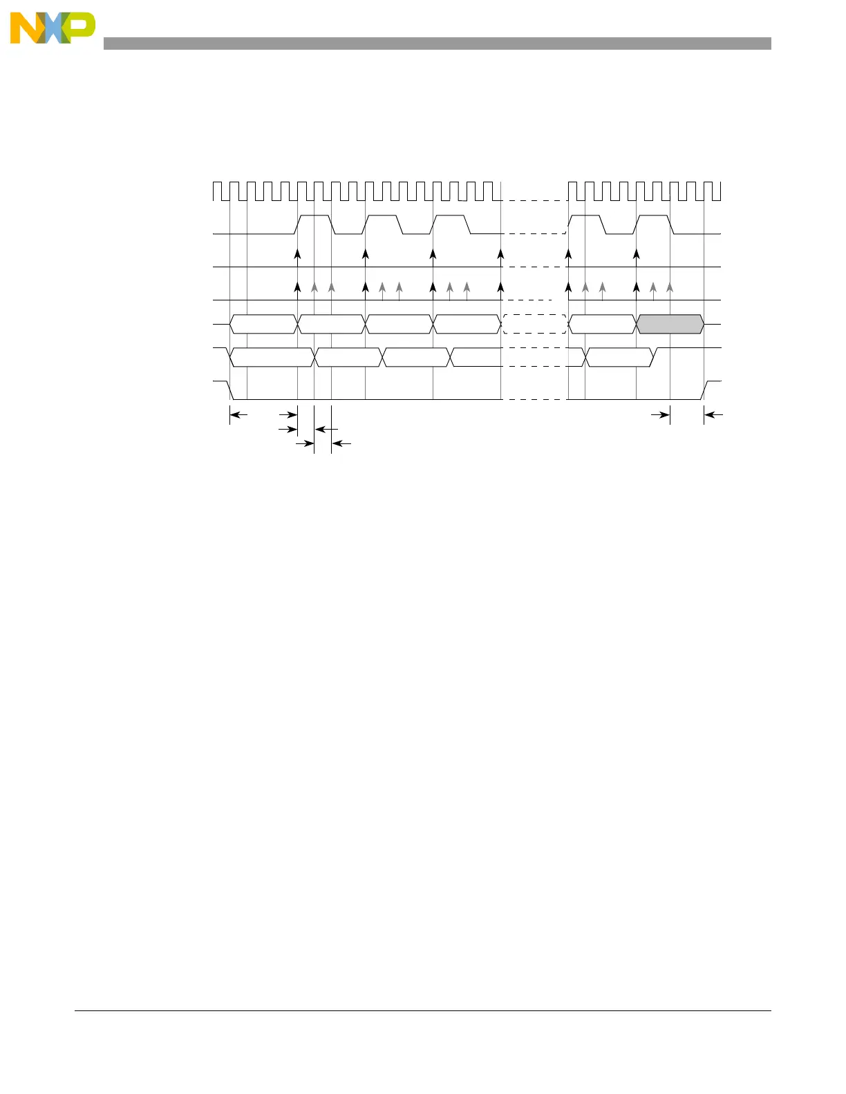
Figure 23-18 shows the modified transfer format for CPHA = 0. Only the condition where CPOL = 0 is
illustrated. The delayed master sample points are indicated with a lighter shaded arrow.
Figure 23-18. DSPI modified transfer format (MTFE = 1, CPHA = 0, f
SCK
= f
SYS
/ 4)
23.6.5.4 Modified SPI transfer format (MTFE = 1, CPHA = 1)
At the start of a transfer the DSPI asserts the CS signal to the slave device. After the CS to SCK delay has
elapsed the master and the slave put data on their SOUT pins at the first edge of SCK. The slave samples
the master SOUT signal on the even numbered edges of SCK. The master samples the slave SOUT signal
on the odd numbered SCK edges starting with the third SCK edge. The slave samples the last bit on the
last edge of the SCK. The master samples the last slave SOUT bit one half SCK cycle after the last edge
of SCK. No clock edge is visible on the master SCK pin during the sampling of the last bit. The SCK to
CS delay must be greater or equal to half of the SCK period.
NOTE
For the modified transfer format to operate correctly, you must thoroughly
analyze the SPI link timing budget.
t
CSC
= CS to SCK delay.
t
ASC
= After SCK delay.
System clock
123456
CSx
t
ASC
SCK
Master sample
Slave SOUT
Master SOUT
System clock
System clock
Slave sample
t
CSC