MPC5604B/C Microcontroller Reference Manual, Rev. 8
Freescale Semiconductor 693
27.5.2.4 DFlash Low/Mid Address Space Block Select Register (DFLASH_LMS)
The DFLASH_LMS register provides a means to select blocks to be operated on during erase.
27.5.2.5 DFlash Address Register (DFLASH_ADR)
The DFLASH_ADR provides the first failing address in the event module failures (ECC, RWW or FPEC)
occur or the first address at which an ECC single error correction occurs.
Offset: 0x00010 Access: Read/write
0123456789101112131415
R
0000000000000000
W
Reset
0000000000000000
16 17 18 19 20 21 22 23 24 25 26 27 28 29 30 31
R
000000000000
LSL
W
Reset
0000000000000000
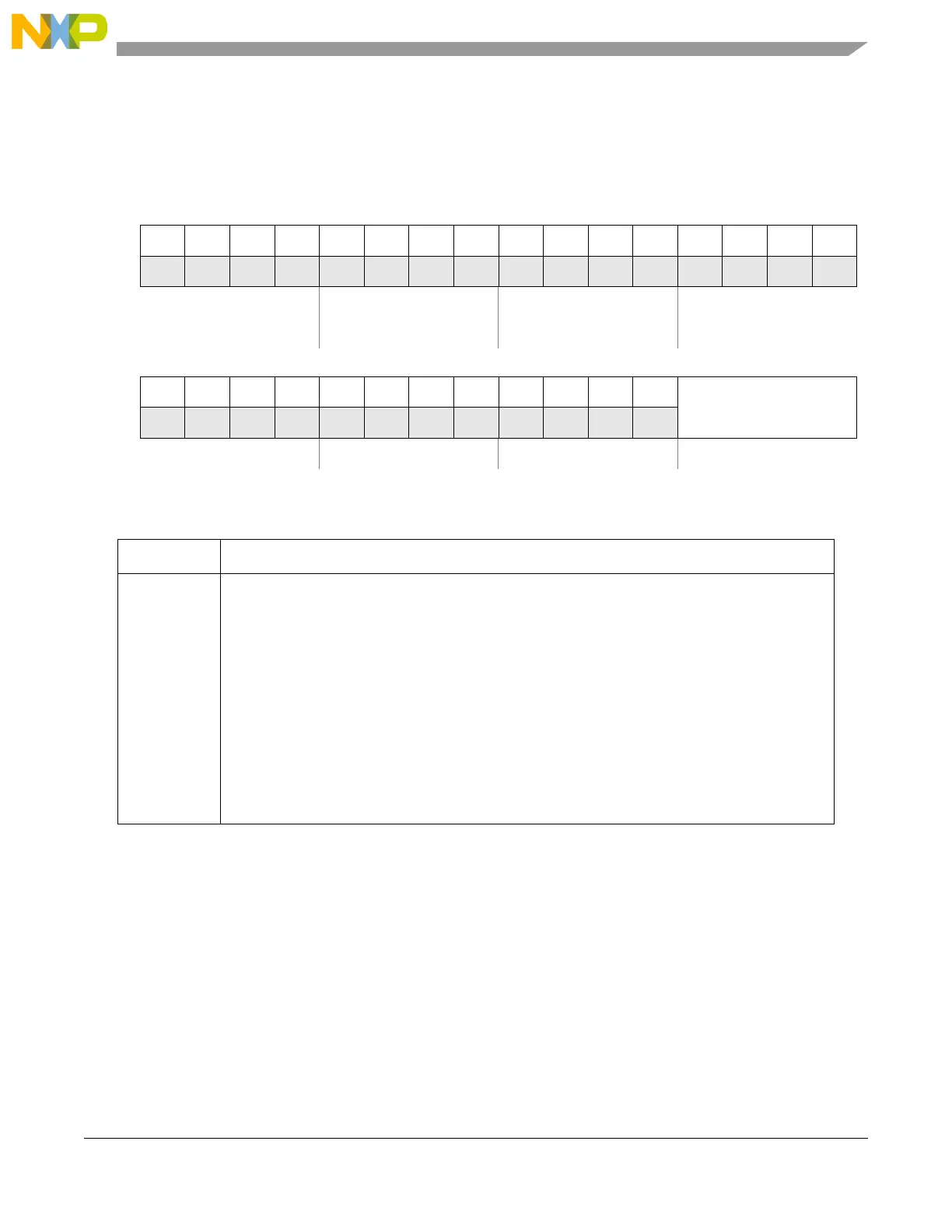
Figure 27-28. DFlash Low/Mid Address Space Block Select Register (DFLASH_LMS)
Table 27-43. DFLASH_LMS field descriptions
Field Description
LSL Low address space block SeLect
A value of 1 in the select register signifies that the block is selected for erase.
A value of 0 in the select register signifies that the block is not selected for erase. The reset value
for the select register is 0, or unselected.
LSL[3:0] are related to sectors B1F3-0, respectively. LSL[15:4] are not used for this memory cut.
The blocks must be selected (or unselected) before doing an erase interlock write as part of the
erase sequence. The select register is not writable once an interlock write is completed or if a high
voltage operation is suspended.
In the event that blocks are not present (due to configuration or total memory size), the
corresponding LSL bits will default to unselected, and will not be writable. The reset value will
always be 0, and register writes will have no effect.
In the 80 KB flash memory module bits LSL[15:4] are read-only and locked at ‘0’.
0: Low Address Space Block is unselected for Erase.
1: Low Address Space Block is selected for Erase.