MPC5604B/C Microcontroller Reference Manual, Rev. 8
344 Freescale Semiconductor
CAUTION
Toggling several IOs at the same time can significantly increase the current in a pad group. Caution must
be taken to avoid exceeding maximum current thresholds. Please see data sheet.
19.5.3.11 GPIO Pad Data Input Registers (GPDI0_3–GPDI120_123)
These registers are used to read the GPIO pad data with a byte access.
Offsets: 0x0600–0x0678 (31 registers) Access: User read/write
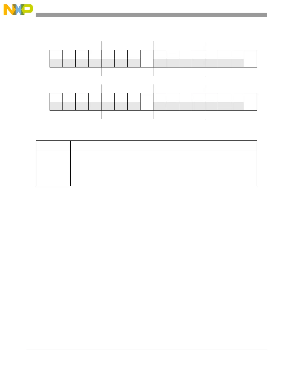
0123456789101112131415
R0000000
PDO[0]
0000000
PDO[1]
W
Reset0000000000000000
16 17 18 19 20 21 22 23 24 25 26 27 28 29 30 31
R0000000
PDO[2]
0000000
PDO[3]
W
Reset0000000000000000
Figure 19-11. Port GPIO Pad Data Output Register 0–3 (GPDO0_3)
Table 19-14. GPDO0_3 field descriptions
Field Description
PDO[x] Pad Data Out
This bit stores the data to be driven out on the external GPIO pad controlled by this register.
0 Logic low value is driven on the corresponding GPIO pad when the pad is configured as an
output
1 Logic high value is driven on the corresponding GPIO pad when the pad is configured as an
output