MPC5604B/C Microcontroller Reference Manual, Rev. 8
Freescale Semiconductor 345
19.5.3.12 Parallel GPIO Pad Data Out Registers (PGPDO0 – PGPDO3)
MPC5604B devices ports are constructed such that they contain 16 GPIO pins, for example PortA[0..15].
Parallel port registers for input (PGPDI) and output (PGPDO) are provided to allow a complete port to be
written or read in one operation, dependent on the individual pad configuration.
Writing a parallel PGPDO register directly sets the associated GPDO register bits. There is also a masked
parallel port output register allowing the user to determine which pins within a port are written.
While very convenient and fast, this approach does have implications regarding current consumption for
the device power segment containing the port GPIO pads. Toggling several GPIO pins simultaneously can
significantly increase current consumption.
CAUTION
Caution must be taken to avoid exceeding maximum current thresholds
when toggling multiple GPIO pins simultaneously. Please see data sheet.
Table 19-16 shows the locations and structure of the PGPDOx registers.
Offsets: 0x0800–0x0878 (31 registers) Access: User read
0123456789101112131415
R
0000000
PDI[0]
0000000
PDI[1]
W
Reset0000000000000000
16 17 18 19 20 21 22 23 24 25 26 27 28 29 30 31
R
0000000
PDI[2]
0000000
PDI[3]
W
Reset0000000000000000
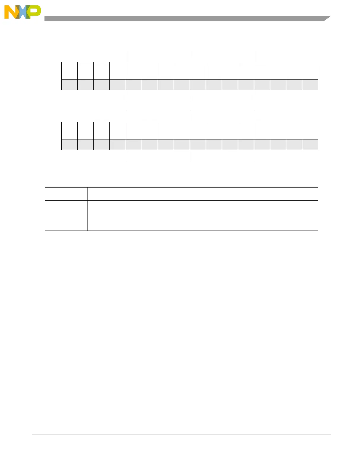
Figure 19-12. Port GPIO Pad Data Input Register 0–3 (GPDI0_3)
Table 19-15. GPDI0_3 field descriptions
Field Description
PDI[x] Pad Data In
This bit stores the value of the external GPIO pad associated with this register.
0 Value of the data in signal for the corresponding GPIO pad is logic low
1 Value of the data in signal for the corresponding GPIO pad is logic high