MPC5604B/C Microcontroller Reference Manual, Rev. 8
346 Freescale Semiconductor
It is important to note the bit ordering of the ports in the parallel port registers. The most significant bit of
the parallel port register corresponds to the least significant pin in the port.
For example in Table 19-16, the PGPDO0 register contains fields for Port A and Port B.
• Bit 0 is mapped to Port A[0], bit 1 is mapped to Port A[1] and so on, through bit 15, which is
mapped to Port A[15]
• Bit 16 is mapped to Port B[0], bit 17 is mapped to Port B[1] and so on, through bit 31, which is
mapped to Port B[15].
19.5.3.13 Parallel GPIO Pad Data In Registers (PGPDI0 – PGPDI3)
The SIU_PGPDI registers are similar in operation to the PGPDIO registers, described in the previous
section (Section 19.5.3.12, “Parallel GPIO Pad Data Out Registers (PGPDO0 – PGPDO3)) but they are
used to read port pins simultaneously.
NOTE
The port pins to be read need to be configured as inputs but even if a single
pin within a port has IBE set, then you can still read that pin using the
parallel port register. However, this does mean you need to be very careful.
Reads of PGPDI registers are equivalent to reading the corresponding GPDI registers but significantly
faster since as many as two ports can be read simultaneously with a single 32-bit read operation.
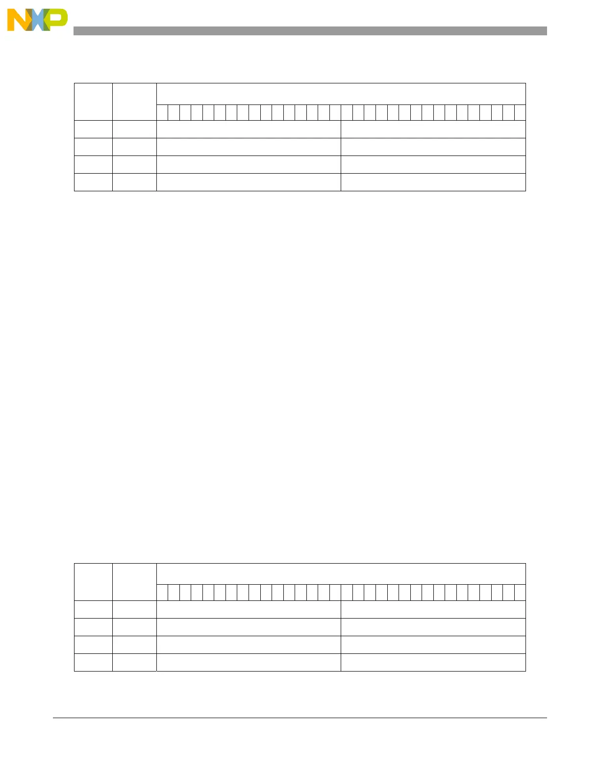
Table 19-17 shows the locations and structure of the PGPDIx registers. Each 32-bit PGPDIx register
contains two 16-bit fields, each field containing the values for a separate port.
Table 19-16. PGPDO0 – PGPDO3 register map
Offset
1
1
SIU base address is 0xC3F9_0000. To calculate register address add offset to base address
Register
Field
0
1
2
3
4
5
6
7
8
9
10
11
12
13
14
15
16
17
18
19
20
21
22
23
24
25
26
27
28
29
30
31
0x0C00 PGPDO0 Port A Port B
0x0C04 PGPDO1 Port C Port D
0x0C08 PGPDO2 Port E Port F
0x0C0C PGPDO3 Port G Port H
Table 19-17. PGPDI0 – PGPDI3 register map
Offset
1
Register
Field
0
1
2
3
4
5
6
7
8
9
10
11
12
13
14
15
16
17
18
19
20
21
22
23
24
25
26
27
28
29
30
31
0x0C40 PGPDI0 Port A Port B
0x0C44 PGPDI1 Port C Port D
0x0C48 PGPDI2 Port E Port F
0x0C4C PGPDI3 Port G Port H