MPC5604B/C Microcontroller Reference Manual, Rev. 8
Freescale Semiconductor 347
It is important to note the bit ordering of the ports in the parallel port registers. The most significant bit of
the parallel port register corresponds to the least significant pin in the port.
For example in Table 19-17, the PGPDI0 register contains fields for Port A and Port B.
• Bit 0 is mapped to Port A[0], bit 1 is mapped to Port A[1] and so on, through bit 15, which is
mapped to Port A[15]
• Bit 16 is mapped to Port B[0], bit 17 is mapped to Port B[1] and so on, through bit 31, which is
mapped to Port B[15].
19.5.3.14 Masked Parallel GPIO Pad Data Out Register (MPGPDO0–MPGPDO7)
The MPGPDOx registers are similar in operation to the PGPDOx ports described in Section 19.5.3.12,
“Parallel GPIO Pad Data Out Registers (PGPDO0 – PGPDO3), but with two significant differences:
• The MPGPDOx registers support masked port-wide changes to the data out on the pads of the
respective port. Masking effectively allows selective bitwise writes to the full 16-bit port.
• Each 32-bit MPGPDOx register is associated to only one port.
NOTE
The MPGPDOx registers may only be accessed with 32-bit writes. 8-bit or
16-bit writes will not modify any bits in the register and will cause a transfer
error response by the module. Read accesses return ‘0’.
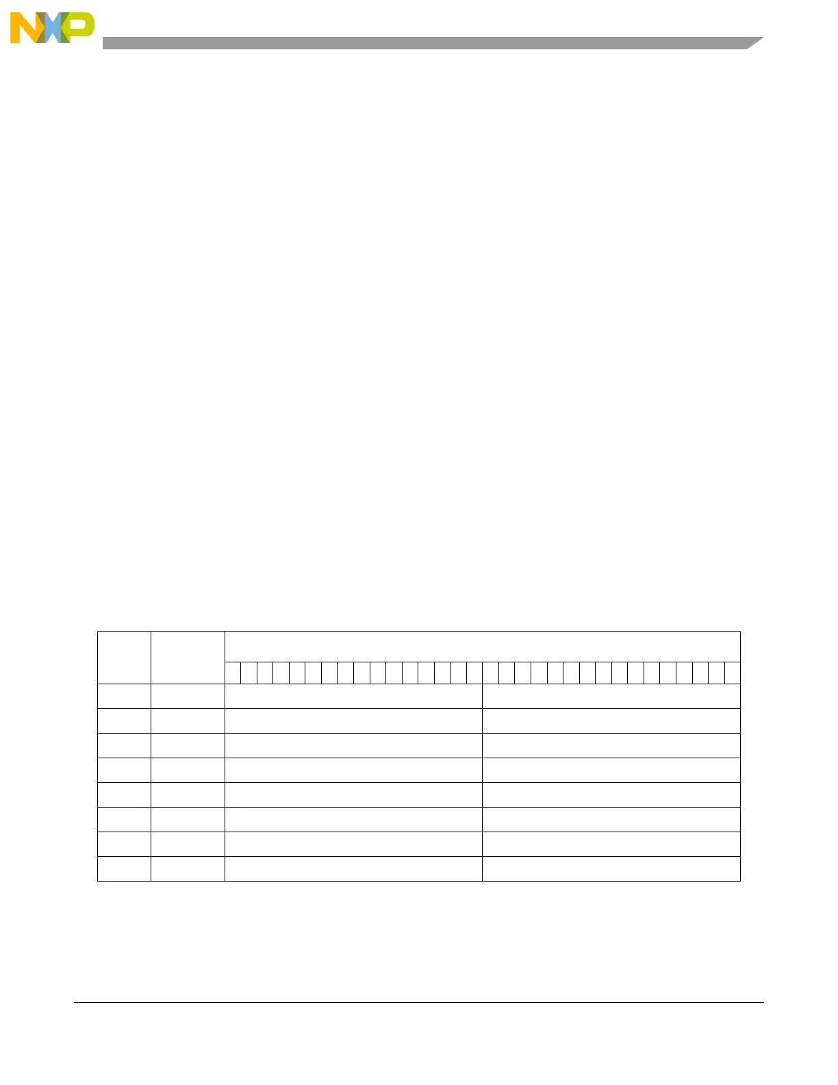
Table 19-18 shows the locations and structure of the MPGPDOx registers. Each 32-bit MPGPDOx register
contains two 16-bit fields (MASK
x
and MPPDO
x
). The MASK field is a bitwise mask for its associated
port. The MPPDO0 field contains the data to be written to the port.
It is important to note the bit ordering of the ports in the parallel port registers. The most significant bit of
the parallel port register corresponds to the least significant pin in the port.
1
SIU base address is 0xC3F9_0000. To calculate register address add offset to base address
Table 19-18. MPGPDO0 – MPGPDO7 register map
Offset
1
1
SIU base address is 0xC3F9_0000. To calculate register address add offset to base address
Register
Field
0
1
2
3
4
5
6
7
8
9
10
11
12
13
14
15
16
17
18
19
20
21
22
23
24
25
26
27
28
29
30
31
0x0C80 MPGPDO0 MASK0 (Port A) MPPDO0 (Port A)
0x0C84 MPGPDO1 MASK1 (Port B) MPPDO1 (Port B)
0x0C88 MPGPDO2 MASK2 (Port C) MPPDO2 (Port C)
0x0C8C MPGPDO3 MASK3 (Port D) MPPDO3 (Port D)
0x0C90 MPGPDO4 MASK4 (Port E) MPPDO4 (Port E)
0x0C94 MPGPDO5 MASK5 (Port F) MPPDO5 (Port F)
0x0C98 MPGPDO6 MASK6 (Port G) MPPDO6 (Port G)
0x0C9C MPGPDO7 MASK7 (Port H) MPPDO7 (Port H)