MPC5604B/C Microcontroller Reference Manual, Rev. 8
Freescale Semiconductor 529
24.3.3.2 Register descriptions
The following sections detail the individual registers within the STM programming model.
24.3.3.2.1 STM Control Register (STM_CR)
The STM Control Register (STM_CR) includes the prescale value, freeze control and timer enable bits.
0x0034 STM Channel 2 Interrupt Register (STM_CIR2) on page 531
0x0038 STM Channel 2 Compare Register (STM_CMP2) on page 531
0x003C Reserved
0x0040 STM Channel 3 Control Register (STM_CCR3) on page 530
0x0044 STM Channel 3 Interrupt Register (STM_CIR3) on page 531
0x0048 STM Channel 3 Compare Register (STM_CMP3) on page 531
0x004C–0x3FFF Reserved
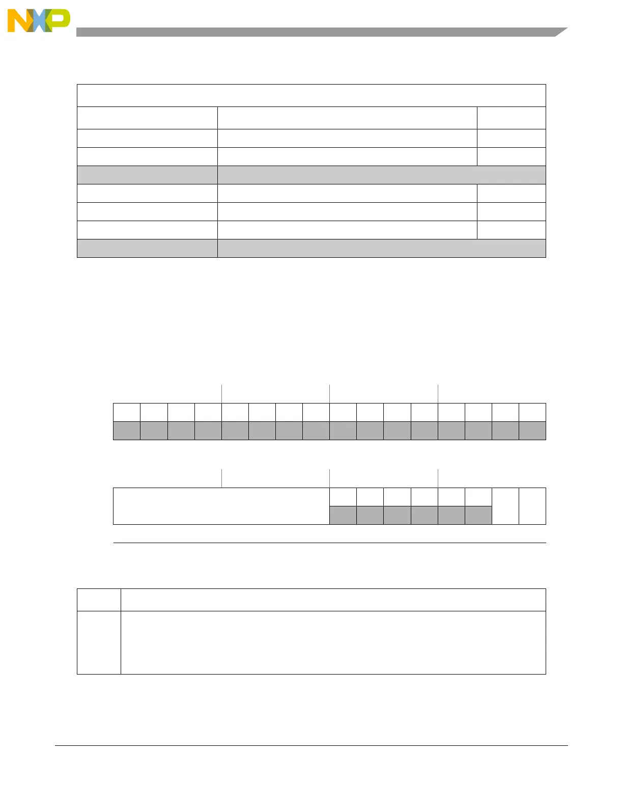
Offset: 0x000 Access: Read/Write
0 1 2 3 4 5 6 7 8 9 101112131415
R 0 0 0 0 0 00000000000
W
Reset0000000000000000
16 17 18 19 20 21 22 23 24 25 26 27 28 29 30 31
R
CPS
0
0 0000
FRZ TEN
W
Reset0000000000000000
Figure 24-2. STM Control Register (STM_CR)
Table 24-4. STM_CR field descriptions
Field Description
CPS Counter Prescaler. Selects the clock divide value for the prescaler (1 - 256).
0x00 = Divide system clock by 1
0x01 = Divide system clock by 2
...
0xFF = Divide system clock by 256
Table 24-3. STM memory map (continued)
Base address: 0xFFF3_C000
Address offset Register Location