MPC5604B/C Microcontroller Reference Manual, Rev. 8
Freescale Semiconductor 539
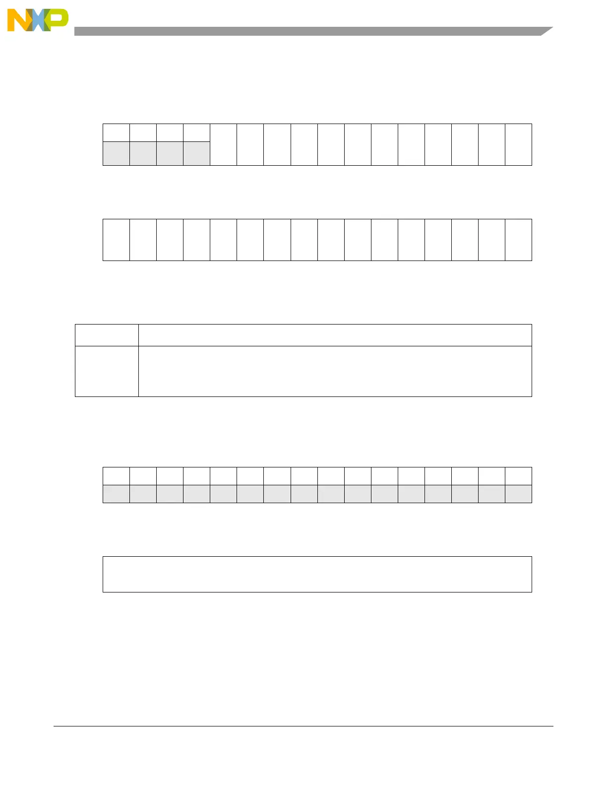
24.4.3.2.4 eMIOS Disable Channel (EMIOSUCDIS) Register
24.4.3.2.5 eMIOS UC A Register (EMIOSA[n])
Depending on the mode of operation, internal registers A1 or A2, used for matches and captures, can be
assigned to address EMIOSA[n]. Both A1 and A2 are cleared by reset. Figure 24-16 summarizes the
EMIOSA[n] writing and reading accesses for all operation modes. For more information see
Section 24.4.4.1.1, UC modes of operation.
Address: eMIOS base address +0x0C
0123456789101112131415
R0000
CHDIS27
CHDIS26
CHDIS25
CHDIS24
CHDIS23
CHDIS22
CHDIS21
CHDIS20
CHDIS19
CHDIS18
CHDIS17
CHDIS16
W
Reset 0/1 0/1 0/1 0/1 0/1 0/1 0/1 0/1 0/1 0/1 0/1 0/1
16 17 18 19 20 21 22 23 24 25 26 27 28 29 30 31
R
CHDIS15
CHDIS14
CHDIS13
CHDIS12
CHDIS11
CHDIS10
CHDIS9
CHDIS8
CHDIS7
CHDIS6
CHDIS5
CHDIS4
CHDIS3
CHDIS2
CHDIS1
CHDIS0
W
Reset0/10/10/10/10/10/10/10/10/10/10/10/10/10/10/10/1
Figure 24-11. eMIOS Enable Channel (EMIOSUCDIS) Register
Table 24-15. EMIOSUCDIS field descriptions
Field Description
CHDISn Enable Channel [n] bit
The CHDIS[n] bit is used to disable each of the channels by stopping its respective clock.
1 = Channel [n] disabled
0 = Channel [n] enabled
Address: UC[n] base address + 0x00
0123456789101112131415
R0000000000000000
W
Reset0000000000000000
16 17 18 19 20 21 22 23 24 25 26 27 28 29 30 31
R
A
W
Reset0000000000000000
Figure 24-12. eMIOS UC A Register (EMIOSA[n])