MPC5604B/C Microcontroller Reference Manual, Rev. 8
Freescale Semiconductor 677
NOTE
In a secured device, starting with a serial boot, it is possible to read the
content of the four flash locations where the RCHW can be stored. For
example if the RCHW is stored at address 0x00000000, the reads at address
0x00000000, 0x00000004, 0x00000008 and 0x0000000C will return a
correct value. Any other flash address cannot be accessed.
27.5.1.16 CFlash Nonvolatile System Censorship Control 0 register (NVSCC0)
The NVSCC0 register stores the 32 LSB of the Censorship Control Word of the device.
The NVSCC0 is a nonvolatile register located in the Shadow sector: it is read during the reset phase of the
flash memory module and the protection mechanisms are activated consequently.
The parts are delivered uncensored to the user.
Table 27-30. NVPWD1 field descriptions
Field Description
PWD[63:32] Password, bits 63–32
These bits represent the 32 MSB of the Private Censorship Password.
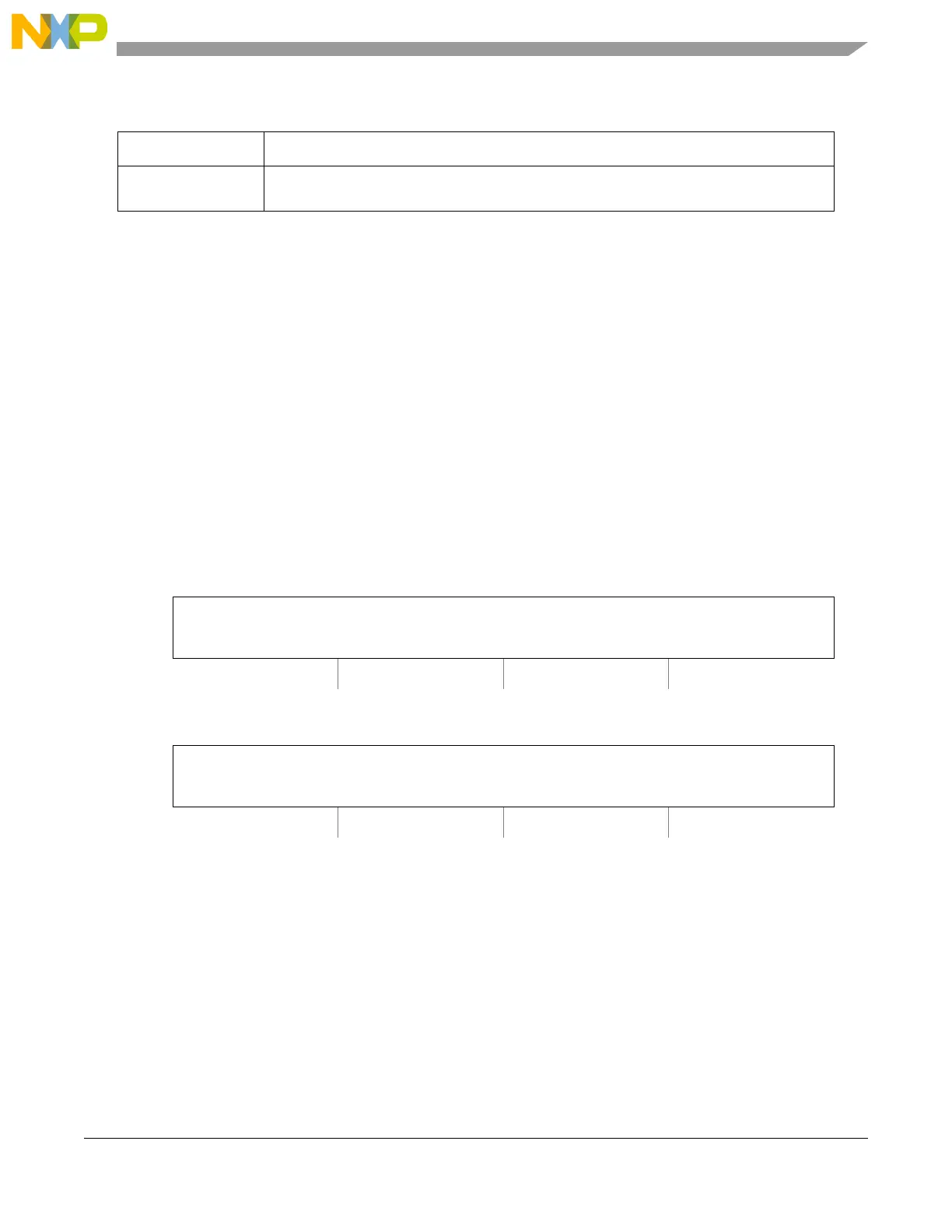
Offset: 0x203DE0 Access: Read/write
0123456789101112131415
R
SC[15:0]
W
Reset
0101010110101010
16 17 18 19 20 21 22 23 24 25 26 27 28 29 30 31
R
CW[15:0]
W
Reset
0101010110101010
Figure 27-20. CFlash Nonvolatile System Censorship Control 0 register (NVSCC0)
 Loading...