MPC5604B/C Microcontroller Reference Manual, Rev. 8
722 Freescale Semiconductor
27.7.2.2.2 Platform Flash Configuration Register 1 (PFCR1)
This register defines the configuration associated with flash memory bank1. This corresponds to the “data
flash memory”. It includes fields that provide specific information for up to two separate AHB ports (p0
and the optional p1). For the platform flash memory controller module, the fields associated with AHB
port p1 are ignored. The register is described below in Figure 27-40 and Table 27-59.
NOTE
Do not execute code from flash memory when you are programming
PFCR1. If you wish to program PFCR1, execute your application code from
RAM.
B0_P0_PFLM Bank0, Port 0 Prefetch Limit
This field controls the prefetch algorithm used by the PFlash controller. This field defines the
prefetch behavior. In all situations when enabled, only a single prefetch is initiated on each buffer
miss or hit. This field is set to 2b10 by hardware reset.
00: No prefetching is performed.
01: The referenced line is prefetched on a buffer miss, that is, prefetch on miss.
1–: The referenced line is prefetched on a buffer miss, or the next sequential page is prefetched on
a buffer hit (if not already present), that is, prefetch on miss or hit.
B0_P0_BFE Bank0, Port 0 Buffer Enable
This bit enables or disables page buffer read hits. It is also used to invalidate the buffers. This bit is
set by hardware reset.
0: The page buffers are disabled from satisfying read requests, and all buffer valid bits are cleared.
1: The page buffers are enabled to satisfy read requests on hits. Buffer valid bits may be set when
the buffers are successfully filled.
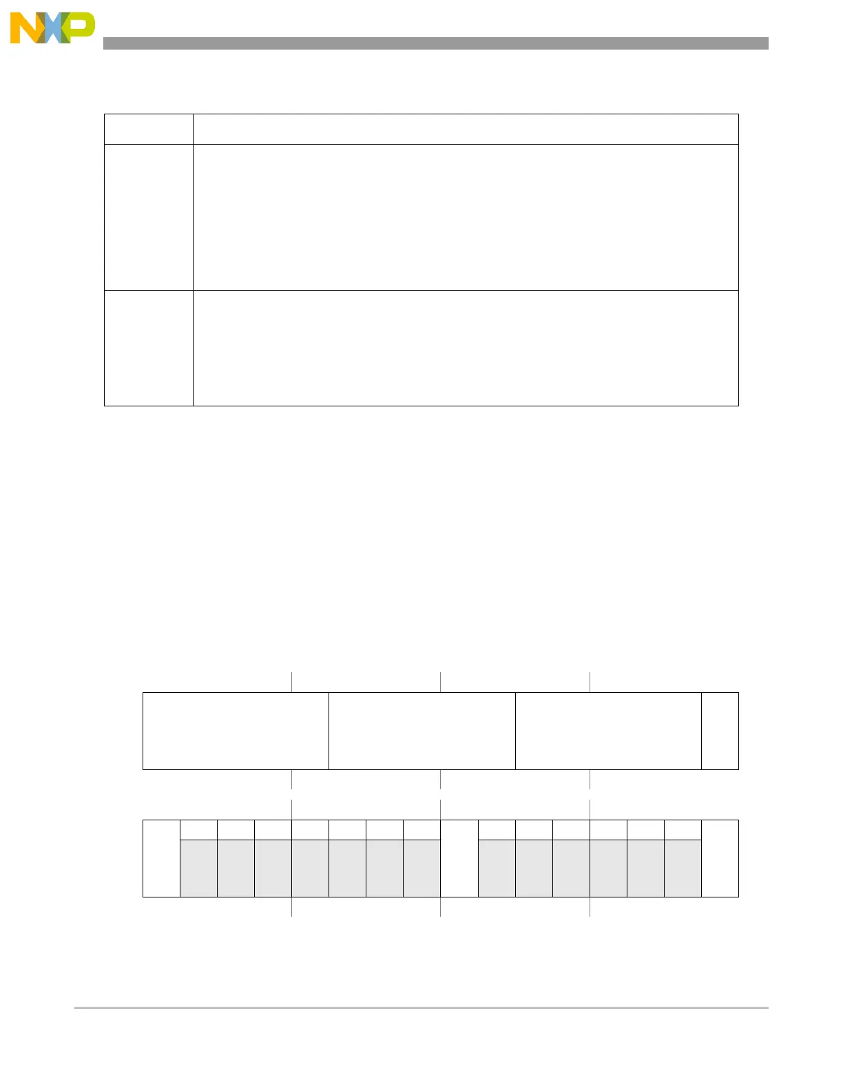
Offset 0x020 Access: Read/write
0123456789101112131415
R
BK1_APC BK1_WWSC BK1_RWSC
BK1_RWWC
W
Reset0001100011000111
16 17 18 19 20 21 22 23 24 25 26 27 28 29 30 31
R
BK1_RWWC
0000000
BK1_RWWC
000000
B1_P0_BFE
W
Reset1000000010000001
Figure 27-40. PFlash Configuration Register 1 (PFCR1)
Table 27-58. PFCR0 field descriptions (continued)
Field Description