MPC5604B/C Microcontroller Reference Manual, Rev. 8
Freescale Semiconductor 747
29.6.2.1 Change lock settings directly via area #4
Memory area #4 contains the lock bits. They can be modified by writing to them. Each SLBRn.SLBm bit
has a mask bit SLBRn.WEm, which protects it from being modified. This masking makes
clear-modify-write operations unnecessary.
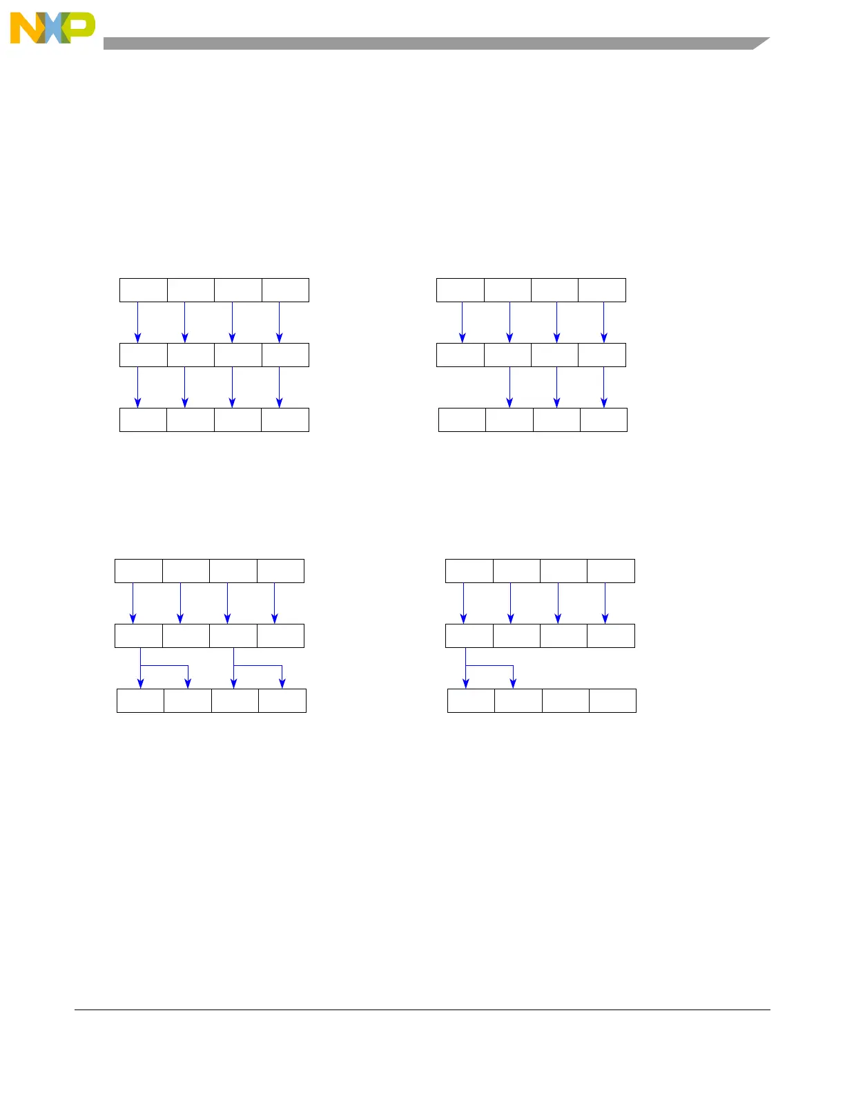
Figure 29-5 shows two modification examples. In the left example there is a write access to the SLBRn
register specifying a mask value which allows modification of all SLBRn.SLBm bits. The example on the
right specifies a mask which only allows modification of the bits SLBRn.SLB[3:1].
Figure 29-5. Change Lock Settings Directly Via Area #4
Figure 29-5 shows four registers that can be protected 8-bit wise. In Figure 29-6 registers with 16-bit
protection and in Figure 29-7 registers with 32-bit protection are shown:
Figure 29-6. Change Lock Settings for 16-bit Protected Addresses
On the right side of Figure 29-6 it is shown that the data written to SLBRn.SLB[0] is automatically written
to SLBRn.SLB[1] also. This is done as the address reflected by SLBRn.SLB[0] is protected 16-bit wise.
Note that in this case the write enable SLBRn.WE[0] must be set while SLBRn.WE[1] does not matter. As
the enable bits SLBRn.WE[3:2] are cleared the lock bits SLBRn.SLB[3:2] remain unchanged.
In the example on the left side of Figure 29-6 the data written to SLBRn.SLB[0] is mirrored to
SLBRn.SLB[1] and the data written to SLBRn.SLB[2] is mirrored to SLBRn.SLB[3] as for both registers
the write enables are set.
1
SLB3SLB2SLB1SLB0
SLBRn.WE[3:0]
SLBRn.SLB[3:0]
SLB3SLB2SLB1SLB0
SLBRn.SLB[3:0]
change allowed
to SLB3
write data
to SLB2to SLB1to SLB0
111
1SLBRn.WE[3:0]
to SLB3
write data
to SLB2to SLB1to SLB0
110
change allowed
SLB0 SLB1 SLB2 SLB3
SLBR
update lock bits
1SLBRn.WE[3:0]
to SLB0
write data
to SLB1 to SLB2 to SLB3
X1X
SLB0 SLB1 SLB2 SLB3
SLBR
update lock bits
1SLBRn.WE[3:0]
to SLB0
write data
to SLB1 to SLB2 to SLB3
X00