MPC5604B/C Microcontroller Reference Manual, Rev. 8
216 Freescale Semiconductor
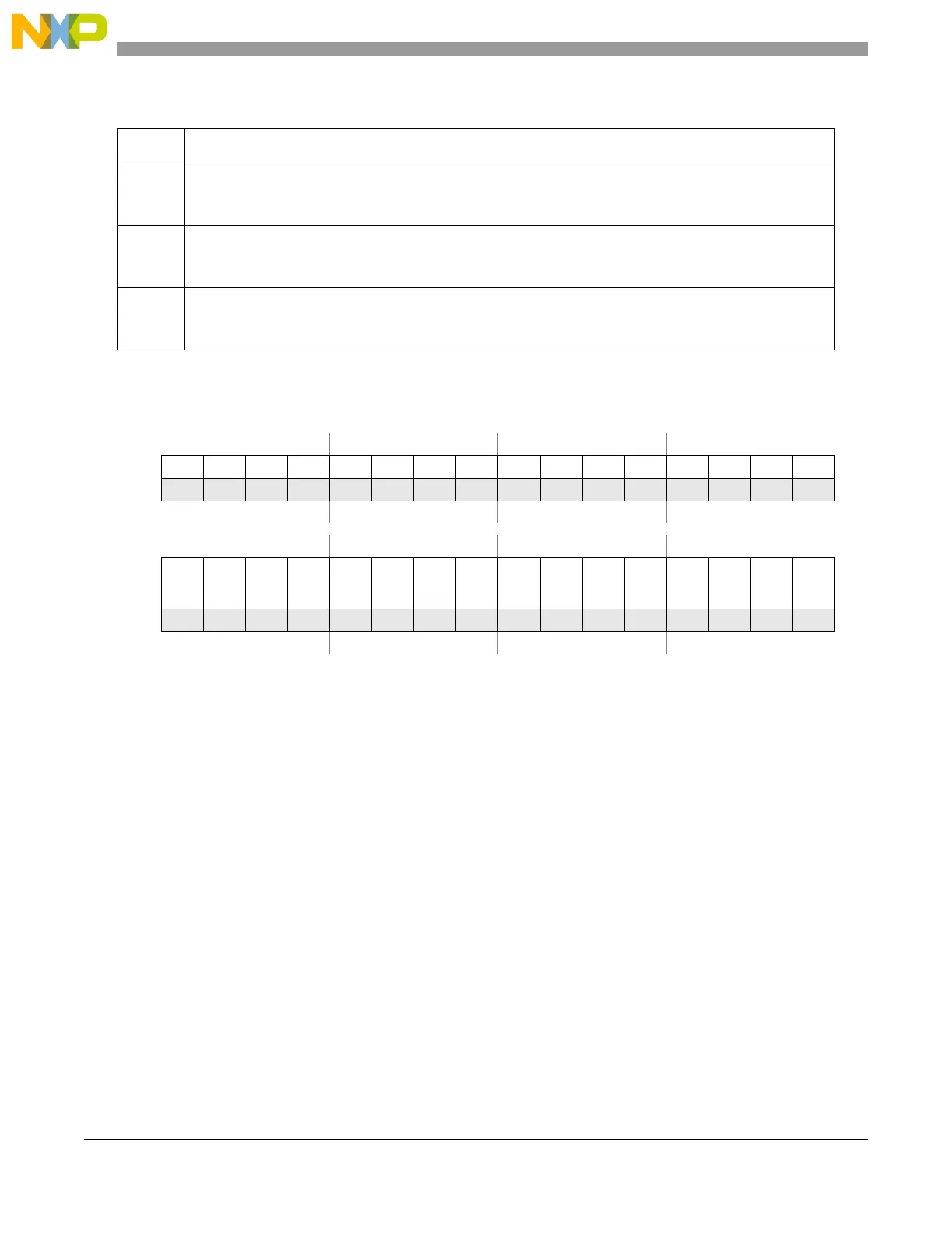
10.3.1.2 Power Domain #1 Configuration Register (PCU_PCONF1)
This register defines for power domain #1 whether it is on or off in each device mode. The bit field
description is the same as in Table 10-3. As the platform, clock generation, and mode control reside in
power domain #1, this power domain is only powered down during the STANDBY mode. Therefore, none
of the bits is programmable. This register is available for completeness reasons.
The difference between PCU_PCONF0 and PCU_PCONF1 is the reset value of the STBY0 bit: During
the STANDBY mode, power domain #1 is disconnected from the power supply, and therefore
PCU_PCONF1.STBY0 is always ‘0’. Power domain #0 is always on, and therefore
PCU_PCONF0.STBY0 is ‘1’.
For further details about STANDBY mode, please see Section 10.4.4.2, “STANDBY Mode Transition.
HALT Power domain control during HALT mode
0 Power domain off
1 Power domain on
STOP Power domain control during STOP mode
0 Power domain off
1 Power domain on
STBY0 Power domain control during STANDBY mode
0 Power domain off
1 Power domain on
Address 0xC3FE_8004 Access: Supervisor read
0123456789101112131415
R0000000000000000
W
Reset0000000000000000
16 17 18 19 20 21 22 23 24 25 26 27 28 29 30 31
R
00
STBY0
00
STOP
0
HALT
RUN3
RUN2
RUN1
RUN0
DRUN
SAFE
TEST
RST
W
Reset0000010111111111
Figure 10-3. Power Domain #1 Configuration Register (PCU_PCONF1)
Table 10-3. Power Domain Configuration Register Field Descriptions (continued)
Field Description