MPC5604B/C Microcontroller Reference Manual, Rev. 8
Freescale Semiconductor 553
Figure 24-25. Input period measurement example
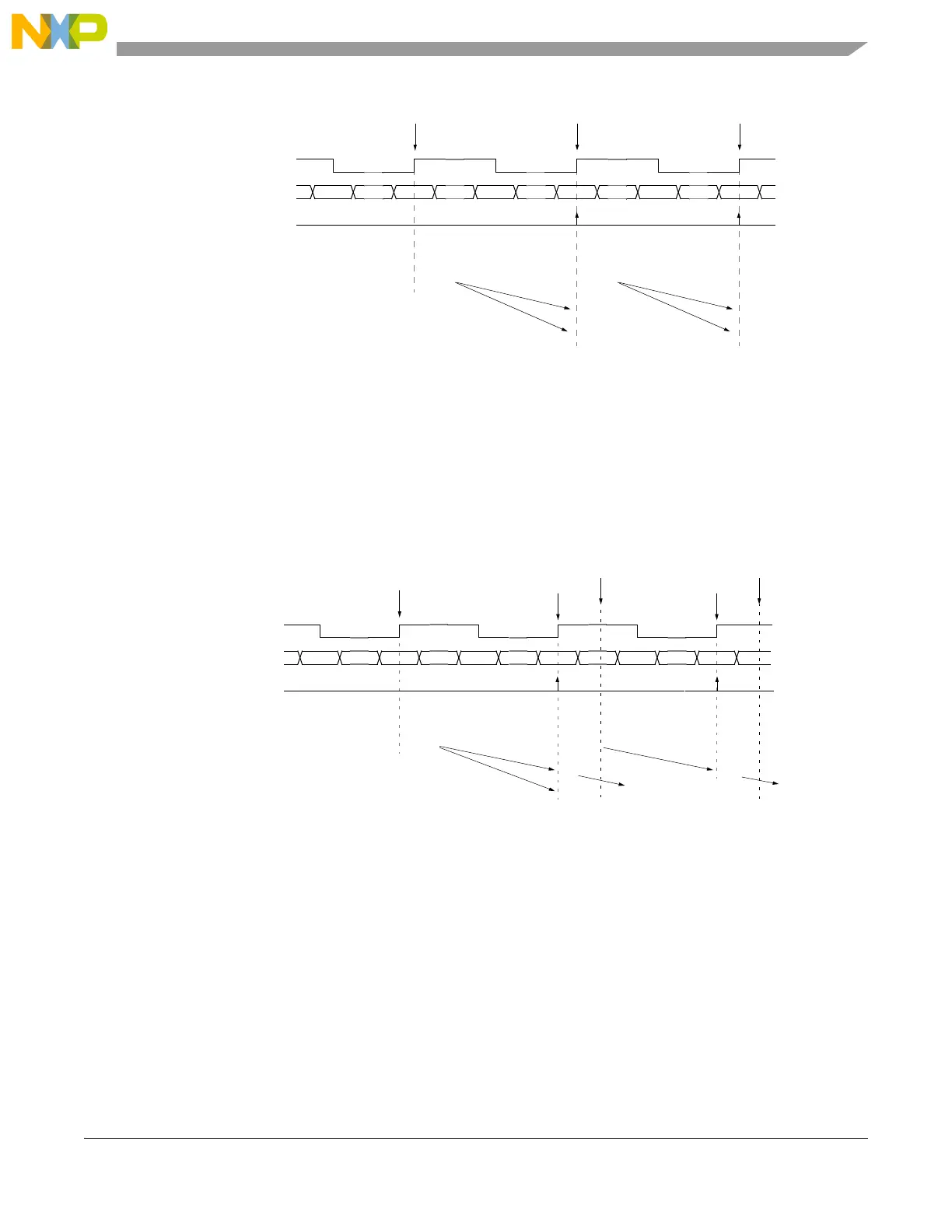
Figure 24-26 describes the A1 and B1 register updates when EMIOSA[n] and EMIOSB[n] read operations
are performed. When EMIOSA[n] read occurs the content of A1 is transferred to B1 thus providing
coherent data in A2 and B1 registers. Transfers from B2 to B1 are then blocked until EMIOSB[n] is read.
After EMIOSB[n] is read, register A1 content is transferred to register B1 and the transfers from B2 to B1
are re-enabled to occur at the transfer edges, which is the leading edge in the Figure 24-26 example.
Figure 24-26. A1 and B1 updates at EMIOSA[n] and EMIOSB[n] reads
24.4.4.1.1.6 Double Action Output Compare (DAOC) mode
In the DAOC mode the leading and trailing edges of the variable pulse width output are generated by
matches occurring on comparators A and B. There is no restriction concerning the order in which A and
B matches occur.
When the DAOC mode is entered, coming out from GPIO mode both comparators are disabled and the
output flip-flop is set to the complement of the EDPOL bit in the EMIOSC[n] register.
selected counter bus 0x000500 0x001000 0x001100 0x001250 0x001525 0x0016A0
A2(captured) value
2
A1 value
B2 (captured) value
0xxxxxxx 0x001000 0x001250
0xxxxxxx 0x001000 0x001250 0x0016A0
0xxxxxxx 0x001000 0x001250 0x0016A0
Input signal
1
EDPOL = 1
FLAG pin register
Notes: 1. After input filter
2. EMIOSA[n] = A2
3. EMIOSB[n] = B1
A A A
B1 value
3
0xxxxxxx 0x001000 0x001250
selected counter bus 0x000500 0x001000 0x001100 0x001250 0x001525 0x0016A0
A2(captured) value
2
B2(captured) value
B1 value
3
0xxxxxxx 0x001000 0x001250 0x0016A0
0xxxxxxx 0x001000
0xxxxxxx 0x001000
Input signal
1
A
AA
FLAG pin/register
EDPOL = 1
A1 value
0xxxxxxx
0x001000
0x001000
0x001250
0x001250
Read EMIOSA[n]
Read EMIOSB[n]
0x001250
Notes: 1. After input filter
2. EMIOSA[n] = A2
3. EMIOSB[n] = B1
0x0016A0