MPC5604B/C Microcontroller Reference Manual, Rev. 8
560 Freescale Semiconductor
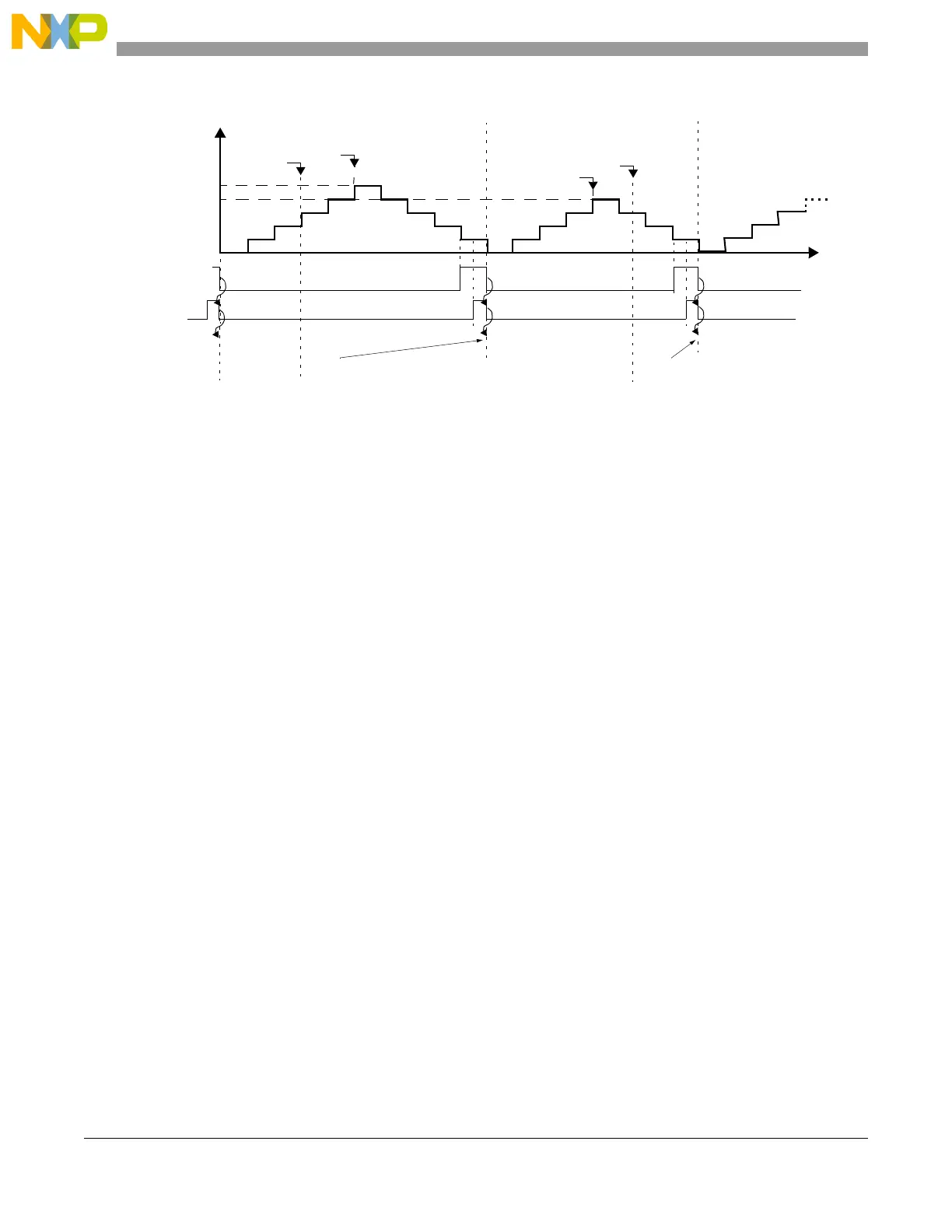
Figure 24-35. MCB Mode A1 Register Update in Up/Down Counter mode
24.4.4.1.1.9 Output Pulse Width and Frequency Modulation Buffered (OPWFMB) mode
This mode (MODE[0:6] = 10110b0) provides waveforms with variable duty cycle and frequency. The
internal channel counter is automatically selected as the time base when this mode is selected. A1 register
indicates the duty cycle and B1 register the frequency. Both A1 and B1 registers are double buffered to
allow smooth signal generation when changing the registers values on the fly. 0% and 100% duty cycles
are supported.
At OPWFMB mode entry the output flip-flop is set to the value of the EDPOL bit in the EMIOSC[n]
register.
If when entering OPWFMB mode coming out from GPIO mode the internal counter value is not within
that range then the B match will not occur causing the channel internal counter to wrap at the maximum
counter value which is 0xFFFF for a 16-bit counter. After the counter wrap occurs it returns to 0x1 and
resume normal OPWFMB mode operation. Thus in order to avoid the counter wrap condition make sure
its value is within the 0x1 to B1 register value range when the OPWFMB mode is entered.
When a match on comparator A occurs the output register is set to the value of EDPOL. When a match on
comparator B occurs the output register is set to the complement of EDPOL. B1 match also causes the
internal counter to transition to 0x1, thus restarting the counter cycle.
Only values greater than 0x1 are allowed to be written to B1 register. Loading values other than those leads
to unpredictable results. If you want to configure the module for OPWFMB mode, ensure that the B1
register is modified before the mode is set.
Figure 24-36 describes the operation of the OPWFMB mode regarding output pin transitions and A1/B1
registers match events. Note that the output pin transition occurs when the A1 or B1 match signal is
deasserted which is indicated by the A1 match negedge detection signal. If register A1 is set to 0x4 the
output pin transitions 4 counter periods after the cycle had started, plus one system clock cycle. Note that
in the example shown in Figure 24-36 the internal counter prescaler has a ratio of two.
A1 value
0x000006
A2 value
0x000006
0x000005
0x000006
0x000005
A1 load signal
Counter = 2
EMIOSCNT[n]
TIME
write to A2
match A1
match A1
write to A2
0x000001
0x000005
0x000006
0x000006
cycle n
cycle n+1
cycle n+2
Prescaler ratio = 2
 Loading...