MPC5604B/C Microcontroller Reference Manual, Rev. 8
570 Freescale Semiconductor
Some rules applicable to the OPWMB mode are:
• B1 matches have precedence over A1 matches if they occur at the same time within the same
counter cycle
• A1 = 0 match from cycle n has precedence over B1 match from cycle n-1
• A1 matches are masked out if they occur after B1 match within the same cycle
• Any value written to A2 or B2 on cycle n is loaded to A1 and B1 registers at the following cycle
boundary (assuming OU[n] bit of EMIOSOUDIS register is not asserted). Thus the new values will
be used for A1 and B1 matches in cycle n+1
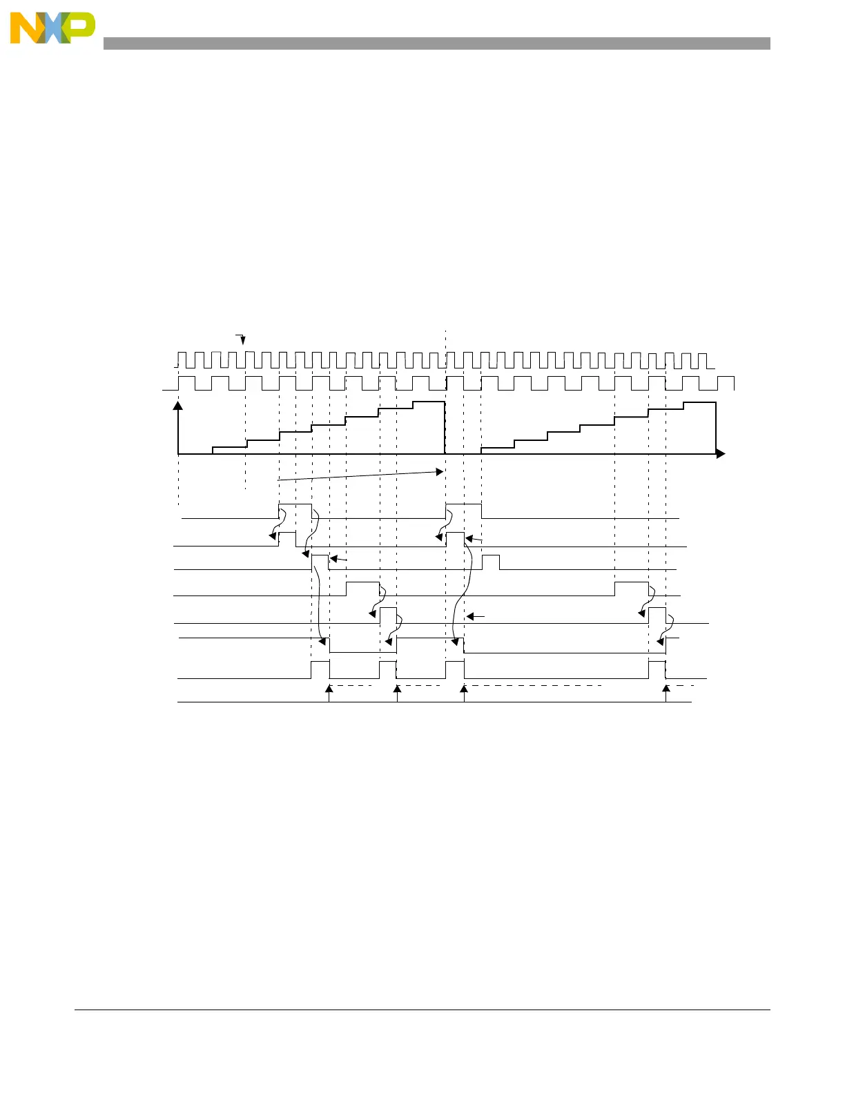
Figure 24-44 describes the operation of the OPWMB mode regarding A1 and B1 matches and the
transition of the channel output pin. In this example EDPOL is set to ‘0’.
Figure 24-44. OPWMB mode matches and flags
Note that the output pin transitions are based on the negedges of the A1 and B1 match signals.
Figure 24-44 shows in cycle n+1 the value of A1 register being set to ‘0’. In this case the match posedge
is used instead of the negedge to transition the output flip-flop.
Figure 24-45 describes the channel operation for 0% duty cycle. Note that the A1 match posedge signal
occurs at the same time as the B1 = 0x8 negedge signal. In this case A1 match has precedence over B1
match, causing the output pin to remain at EDPOL bit value, thus generating a 0% duty cycle signal.
1
4
match A1 negedge detection
6
A1 value 0x000004
A1 match
A1 match negedge detection
output pin
EDPOL = 0
TIME
match B1 negedge detection
B1 match
B1 match negedge detection
B1 value
0x000006
clock
prescaler
A2 value
0x000000
write to A2
0x000000
A1 match posedge detection
match A1 posedge detection
1
cycle n
cycle n+1
8
6
FLAG set event
Selected
counter bus
FLAG pin/register