MPC5604B/C Microcontroller Reference Manual, Rev. 8
Freescale Semiconductor 569
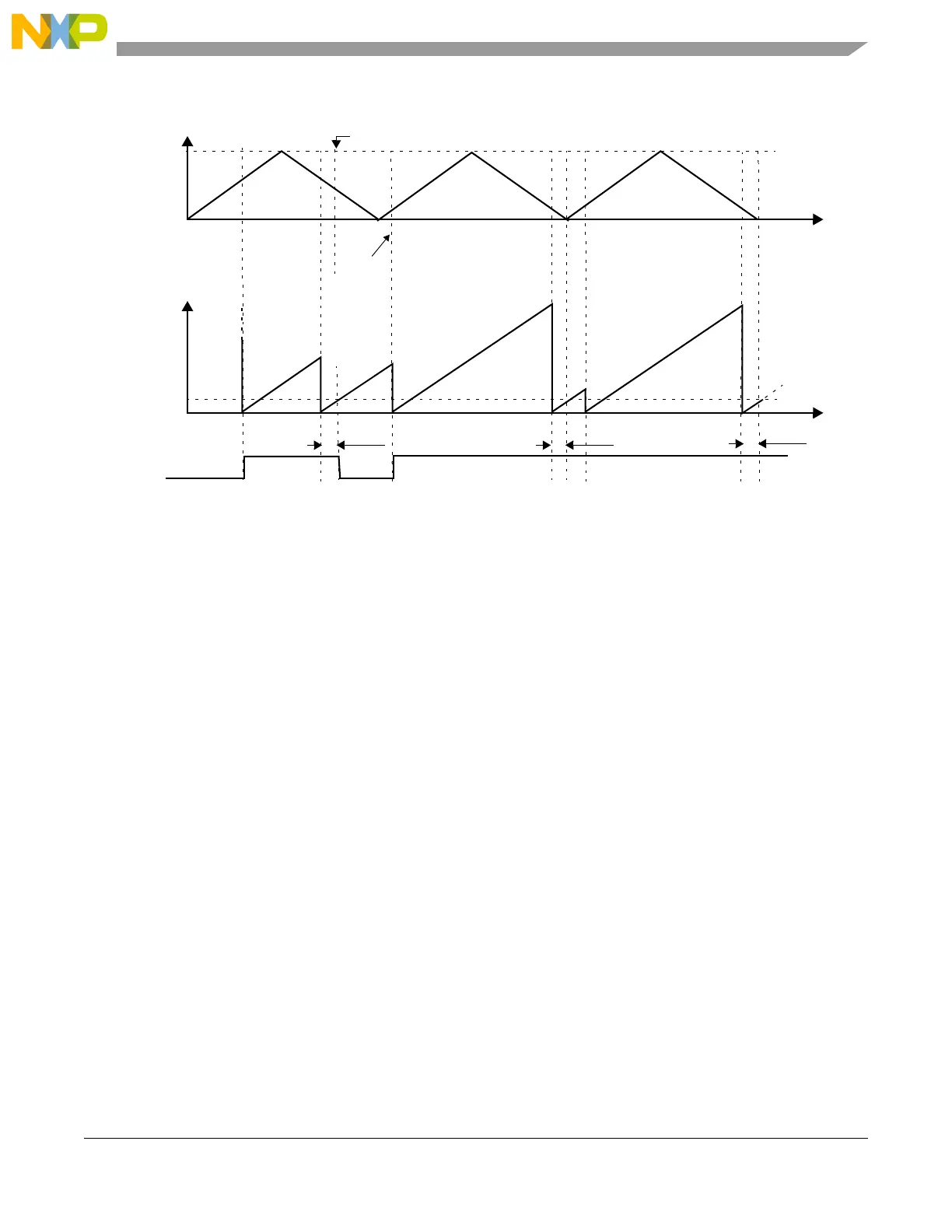
Figure 24-43. OPWMCB with 100% Duty Cycle (A1 = 4 and B1 = 3)
It is important to notice that, such as in OPWMB and OPWFMB modes, the match signal used to set or
clear the channel output flip-flop is generated on the deassertion of the channel combinational comparator
output signal which compares the selected time base with A1 or B1 register values. Please refer to
Figure 24-36 which describes the delay from matches to output flip-flop transition in OPWFMB mode.
The operation of OPWMCB mode is similar to OPWFMB regarding matches and output pin transition.
24.4.4.1.1.11 Output Pulse Width Modulation Buffered (OPWMB) Mode
OPWMB mode (MODE[0:6] = 11000b0) is used to generate pulses with programmable leading and
trailing edge placement. An external counter driven in MCB Up mode must be selected from one of the
counter buses. A1 register value defines the first edge and B1 the second edge. The output signal polarity
is defined by the EDPOL bit. If EDPOL is zero, a negative edge occurs when A1 matches the selected
counter bus and a positive edge occurs when B1 matches the selected counter bus.
The A1 and B1 registers are double buffered and updated from A2 and B2, respectively, at the cycle
boundary. The load operation is similar to the OPWFMB mode. Please refer to Figure 24-38 for more
information about A1 and B1 registers update.
FLAG can be generated at B1 matches, when MODE[5] is cleared, or in both A1 and B1 matches, when
MODE[5] is set. If subsequent matches occur on comparators A and B, the PWM pulses continue to be
generated, regardless of the state of the FLAG bit.
FORCMA and FORCMB bits allow the software to force the output flip-flop to the level corresponding
to a match on A1 or B1 respectively. FLAG bit is not set by the FORCMA and FORCMB operations.
At OPWMB mode entry the output flip-flop is set to the value of the EDPOL bit in the EMIOSC[n]
register.
0x000001
dead time
0x000020
dead time
dead time
write to A2
selected
counter bus
internal
time
base
0x000004
A1 value
A2 value
B1 value
B2 value
0x000004
0x000001
output flip-flop
0x000003
0x000015
0x000003
0x000015
0x000003
cycle n cycle n+1
cycle n+2



 To Next Page