RM0402 Rev 6 355/1163
RM0402 Digital filter for sigma delta modulators (DFSDM)
400
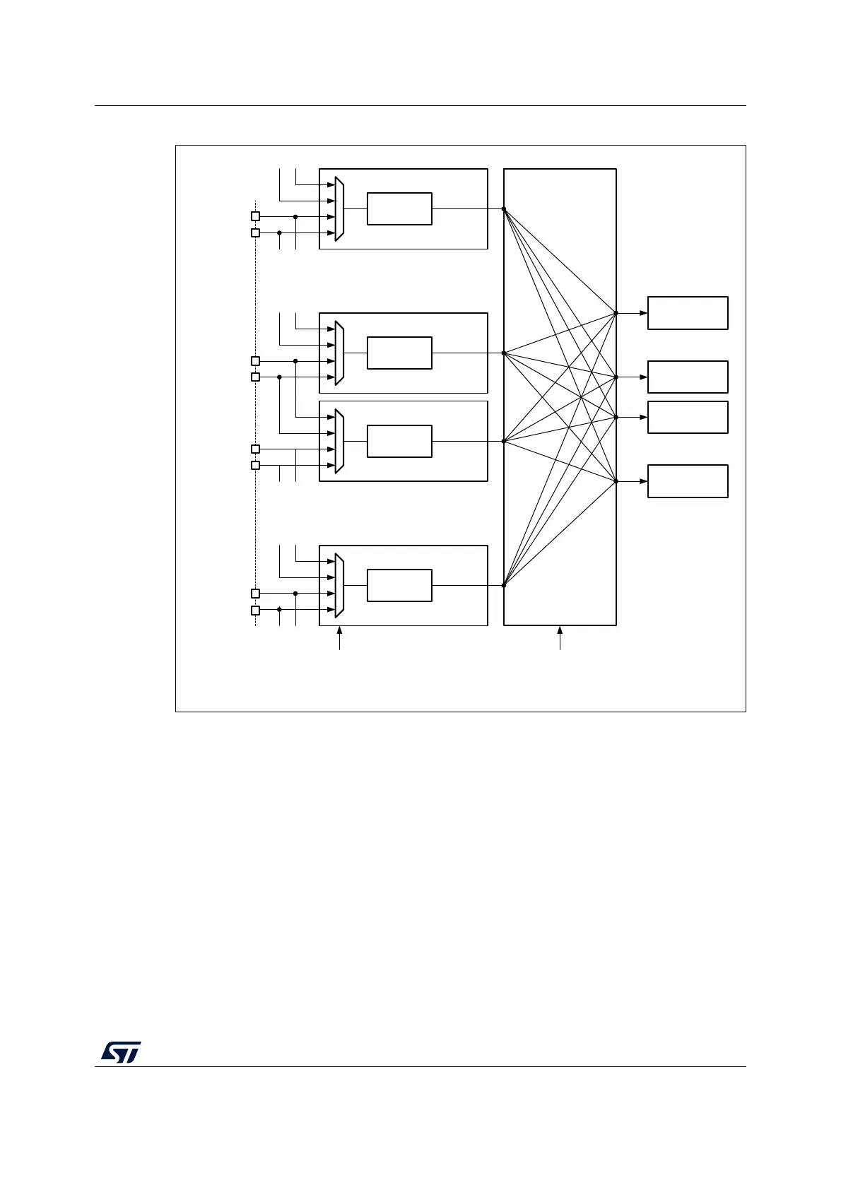
Figure 68. Input channel pins redirection
Output clock generation
A clock signal can be provided on CKOUT pin to drive external Σ∆ modulator clock inputs.
The frequency of this CKOUT signal is derived from DFSDM clock or from audio clock (see
CKOUTSRC bit in DFSDM_CH0CFGR1 register) divided by a predivider (see CKOUTDIV
bits in DFSDM_CH0CFGR1 register). If the output clock is stopped, then CKOUT signal is
set to low state (output clock can be stopped by CKOUTDIV=0 in DFSDM_CHyCFGR1
register or by DFSDMEN=0 in DFSDM_CH0CFGR1 register). The output clock stopping is
performed:
• 4 system clocks after DFSDMEN is cleared (if CKOUTSRC=0)
• 1 system clock and 3 audio clocks after DFSDMEN is cleared (if CKOUTSRC=1)
Before changing CKOUTSRC the software has to wait for CKOUT being stopped to avoid
glitch on CKOUT pin. The output clock signal frequency must be in the range 0 - 20
MHz.
MSv41632V1
FLTx
FLT(x+1)
DATAIN0
DATIN(y-1)
DATINy
DATIN(y
max
)
CHINSEL
RCH
FLT0
FLT(x
max
)
CKIN(y
max
)
CKINy
CKIN(y-1)
CKIN0
.
.
.
.
.
.
CH(y
max
)
Decode
CHy
Decode
CH(y-1)
Decode
.
.
.
CH0
Decode
(. . .)
.
.
.
.
.
.
.
.
.
.
.
.
(. . .)
.
.
.