RM0402 Rev 6 1149/1163
RM0402 Debug support (DBG)
1153
Note: By default, the TRACECLKIN input clock of the TPIU is tied to GND. It is assigned to HCLK
two clock cycles after the bit TRACE_IOEN has been set.
The debugger must then program the Trace Mode by writing the PROTOCOL[1:0] bits in the
SPP_R (Selected Pin Protocol) register of the TPIU.
• PROTOCOL=00: Trace Port Mode (synchronous)
• PROTOCOL=01 or 10: Serial Wire (Manchester or NRZ) Mode (asynchronous mode).
Default state is 01
It then also configures the TRACE port size by writing the bits [3:0] in the CPSPS_R
(Current Sync Port Size Register) of the TPIU:
• 0x1 for 1 pin (default state)
• 0x2 for 2 pins
• 0x8 for 4 pins
30.17.3 TPUI formatter
The formatter protocol outputs data in 16-byte frames:
• seven bytes of data
• eight bytes of mixed-use bytes consisting of:
– 1 bit (LSB) to indicate it is a DATA byte (‘0) or an ID byte (‘1).
– 7 bits (MSB) which can be data or change of source ID trace.
• one byte of auxiliary bits where each bit corresponds to one of the eight mixed-use
bytes:
– if the corresponding byte was a data, this bit gives bit0 of the data.
– if the corresponding byte was an ID change, this bit indicates when that ID change
takes effect.
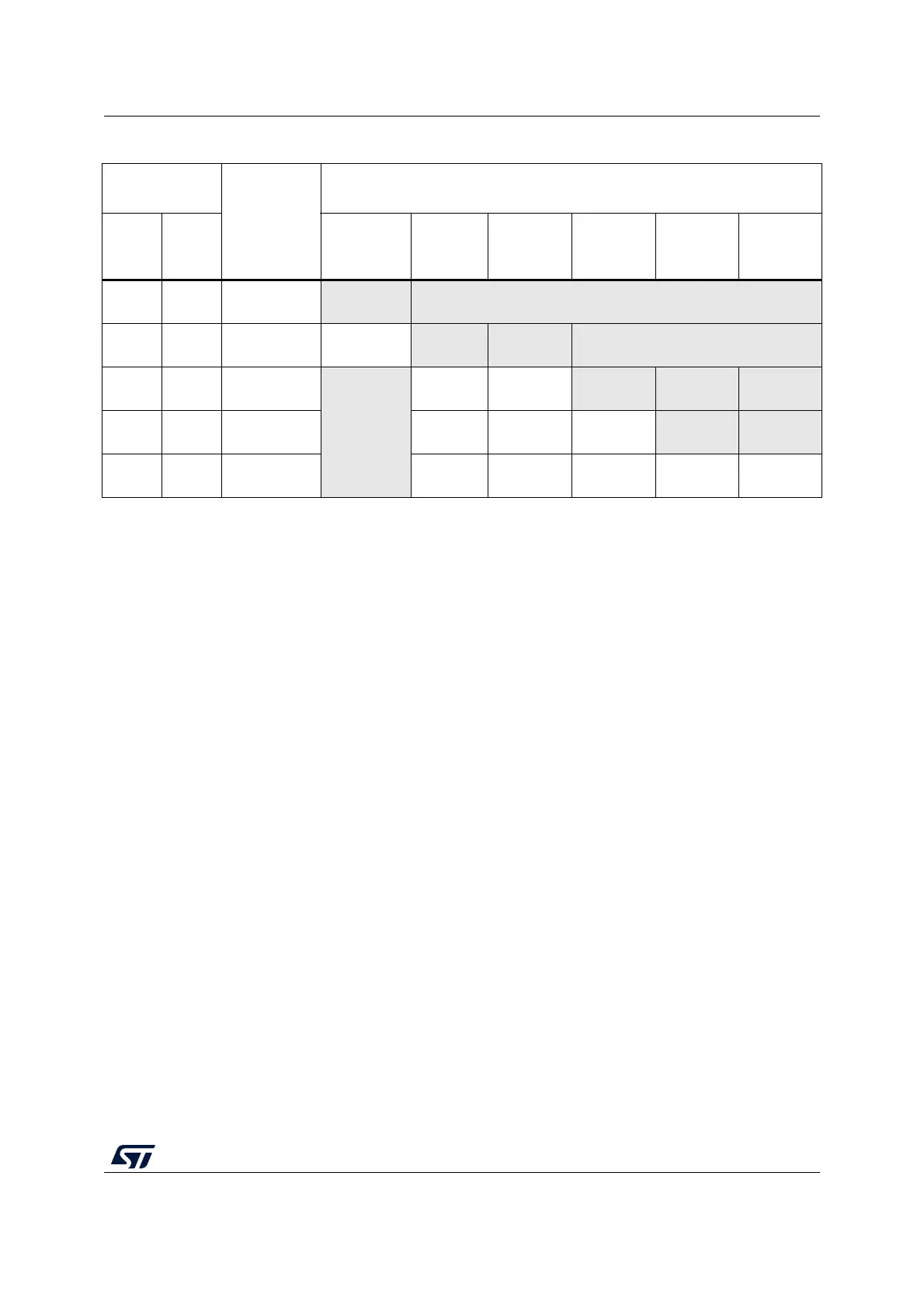
Table 223. Flexible TRACE pin assignment
DBGMCU_CR
register
Pins
assigned for:
TRACE IO pin assigned
(1)
TRACE
_IOEN
TRACE
_MODE
[1:0]
JTDO/
TRACESWO
TRACE
CK
TRACE
D[0]
TRACE
D[1]
TRACE
D[2]
TRACE
D[3]
0XX
No Trace
(default state)
Released
(2)
-
100
Asynchronous
Trace
TRACESWO
- -
Released
(usable as GPIO)
101
Synchronous
Trace 1 bit
Released
(2)
TRACECK TRACED[0] - - -
110
Synchronous
Trace 2 bit
TRACECK TRACED[0] TRACED[1]
- -
111
Synchronous
Trace 4 bit
TRACECK TRACED[0] TRACED[1] TRACED[2] TRACED[3]
1. Refer to the datasheet alternate function mapping table.
2. When Serial Wire mode is used, it is released. But when JTAG is used, it is assigned to JTDO.