RM0402 Rev 6 59/1163
RM0402 Embedded Flash memory interface
81
3.3 Embedded Flash memory
The Flash memory has the following main features:
• Capacity up to 1 Mbyte
• 128 bits wide data read
• Byte, half-word, word and double word write
• Sector and mass erase
• Memory organization
The Flash memory is organized as follows:
– A main memory block divided into 4 sectors of 16 Kbyte, plus 1 sector of 64 Kbyte
and plus 7 sector of 128 Kbyte.
– System memory from which the device boots in System memory boot mode
– 512 OTP (one-time programmable) bytes for user data
The OTP area contains 32 additional bits used to lock the corresponding OTP
data block.
– Option bytes to configure read and write protection, BOR level, watchdog
software/hardware and reset when the device is in Standby or Stop mode.
• Low-power modes (for details refer to the Power control (PWR) section of the reference
manual)
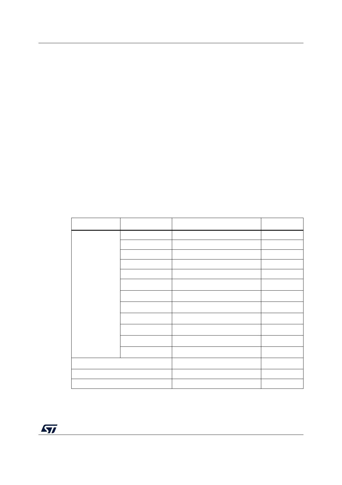
Table 5. Flash module organization
Block Name Block base addresses Size
Main memory
Sector 0 0x0800 0000 - 0x0800 3FFF 16 Kbyte
Sector 1 0x0800 4000 - 0x0800 7FFF 16 Kbyte
Sector 2 0x0800 8000 - 0x0800 BFFF 16 Kbyte
Sector 3 0x0800 C000 - 0x0800 FFFF 16 Kbyte
Sector 4 0x0801 0000 - 0x0801 FFFF 64 Kbyte
Sector 5 0x0802 0000 - 0x0803 FFFF 128 Kbyte
Sector 6 0x0804 0000 - 0x0805 FFFF 128 Kbyte
Sector 7 0x0806 0000 - 0x0807 FFFF 128 Kbyte
Sector 8
(1)
1. Not available for STM32F412xE products
0x0808 0000 - 0x0809 FFFF 128 Kbyte
Sector 9
(1)
0x080A 0000 - 0x080B FFFF 128 Kbyte
Sector 10
(1)
0x080C 0000 - 0x080D FFFF 128 Kbyte
Sector 11
(1)
0x080E 0000 - 0x080F FFFF 128 Kbyte
System memory 0x1FFF 0000 - 0x1FFF 77FF 30 Kbyte
OTP area 0x1FFF 7800 - 0x1FFF 7A0F 528 byte
Option bytes 0x1FFF C000 - 0x1FFF C00F 16 byte