Inter-integrated circuit (I
2
C) interface RM0402
726/1163 RM0402 Rev 6
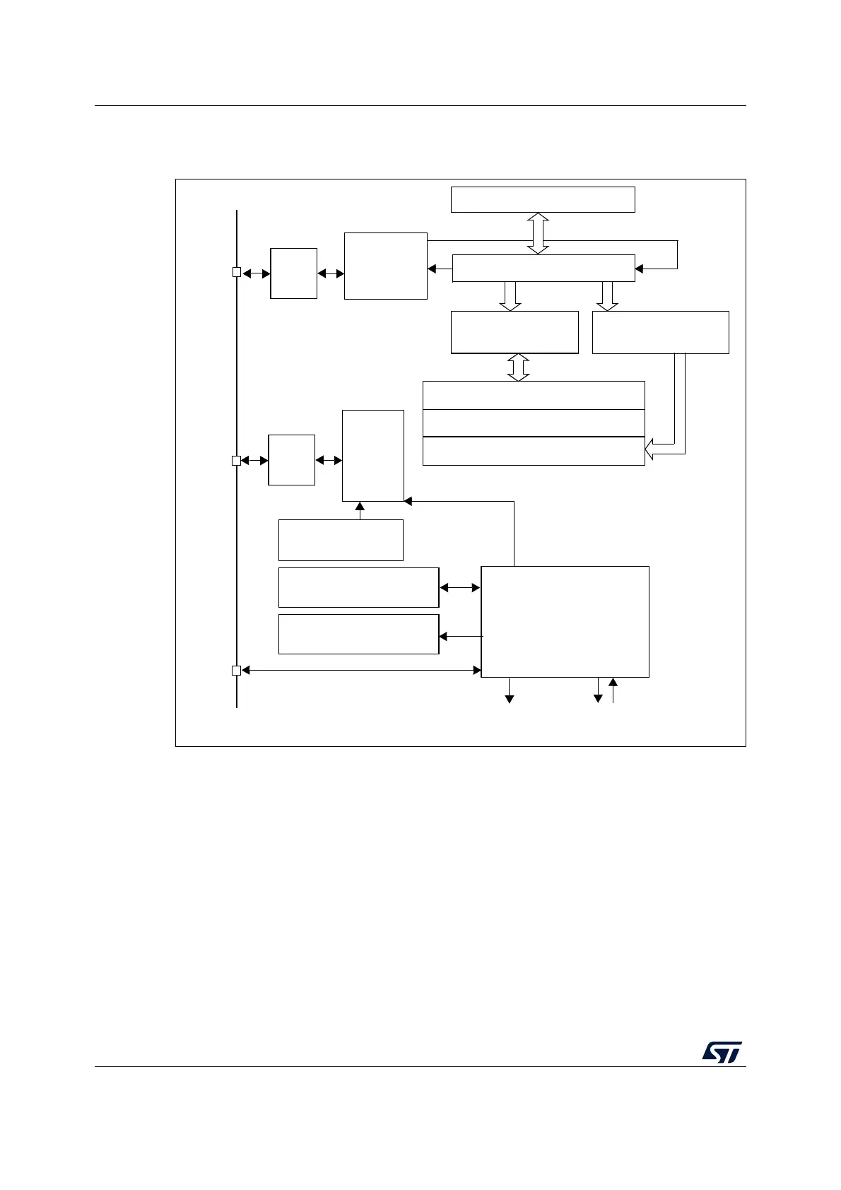
The block diagram of the I
2
C interface is shown in Figure 239.
Figure 239. I
2
C block diagram
1. SMBA is an optional signal in SMBus mode. This signal is not applicable if SMBus is disabled.
24.3.2 I
2
C slave mode
By default the I
2
C interface operates in Slave mode. To switch from default Slave mode to
Master mode a Start condition generation is needed.
The peripheral input clock must be programmed in the I2C_CR2 register in order to
generate correct timings. The peripheral input clock frequency must be at least:
• 2 MHz in Sm mode
• 4 MHz in Fm mode
As soon as a start condition is detected, the address is received from the SDA line and sent
to the shift register. Then it is compared with the address of the interface (OAR1) and with
OAR2 (if ENDUAL=1) or the General Call address (if ENGC = 1).
Data shift register
Comparator
Own address register
Clock control
Status registers
Control registers
Control
Clock
control
Data
control
SCL
logic
Dual address register
Data register
PEC register
Interrupts
PEC calculation
SMBA
SDA
Register (CCR)
(SR1&SR2)
(CR1&CR2)
DMA requests & ACK
MS30035V1
Noise
filter
Noise
filter