RM0402 Rev 6 87/1163
RM0402 Power controller (PWR)
108
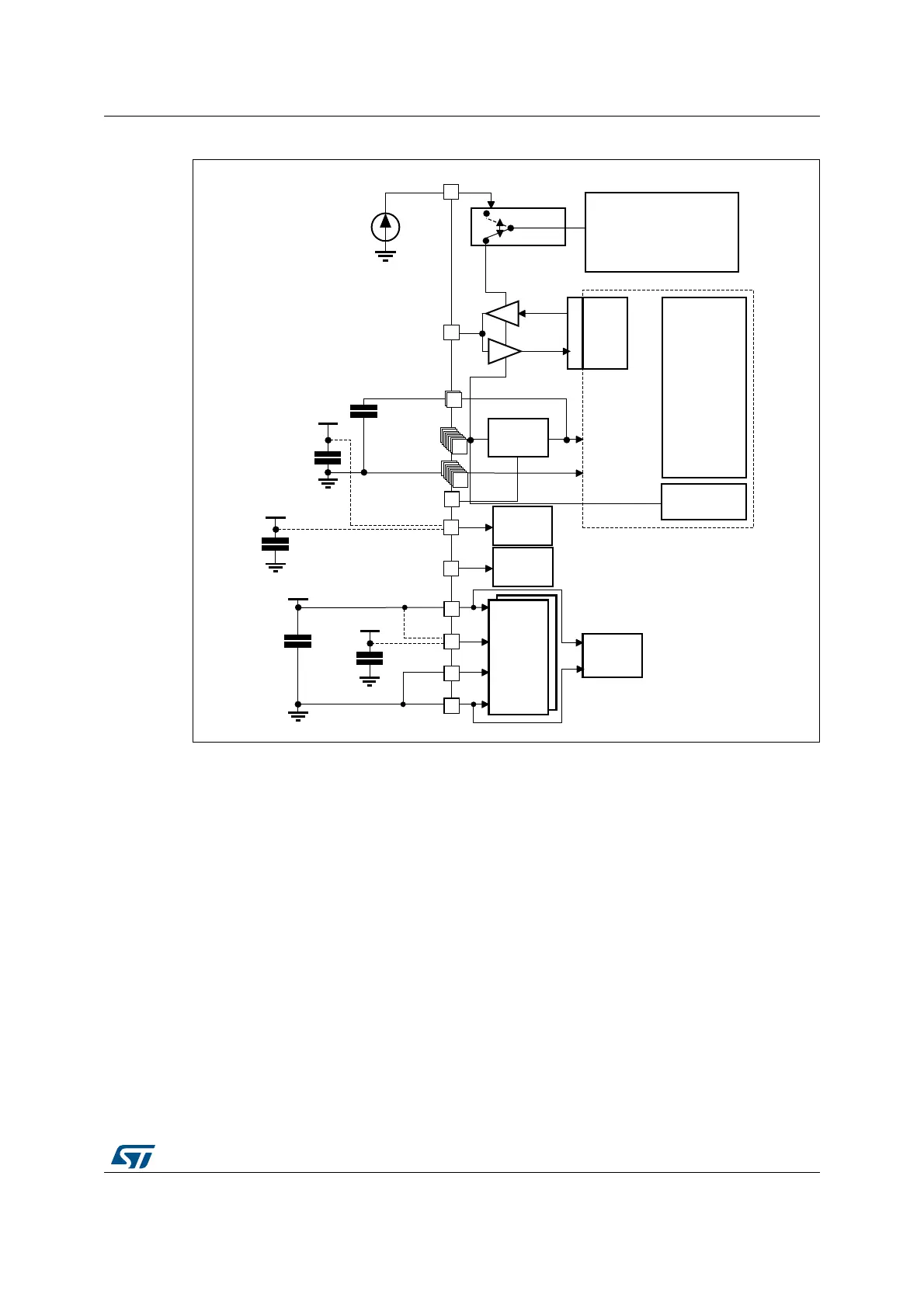
Figure 8. Power supply overview
1. V
DDA
and V
SSA
must be connected to V
DD
and V
SS
, respectively.
5.1.1 Independent A/D converter supply and reference voltage
To improve conversion accuracy, the ADC has an independent power supply which can be
separately filtered and shielded from noise on the PCB.
• The ADC voltage supply input is available on a separate V
DDA
pin.
• An isolated supply ground connection is provided on pin V
SSA
.
To ensure a better accuracy of low voltage inputs, the user can connect a separate external
reference voltage ADC input on V
REF
. The voltage on V
REF
ranges from 1.7 V to V
DDA
.
5.1.2 Battery backup domain
Backup domain description
To retain the content of the RTC backup registers and supply the RTC when V
DD
is turned
off, V
BAT
pin can be connected to an optional standby voltage supplied by a battery or by
another source.
MSv39022V1
Backup circuitry
(OSC32K,RTC,
Wakeup logic
Backup registers)
Kernel logic
(CPU, digital
& RAM)
Analog:
RCs,
PLL,..
Power
switch
V
BAT
GPIOs
OUT
IN
11 × 100 nF
+ 1 × 4.7 μF
V
BAT
=
1.65 to 3.6V
Voltage
regulator
V
DDA
ADC
Level shifter
IO
Logic
V
DD
100 nF
+ 1 μF
Flash memory
V
CAP_1
V
CAP_2
2 × 2.2 μF
BYPASS_REG
PDR_ON
Reset
controller
V
DD
1/2/...11/12
V
SS
1/2/...11/12
V
DD
V
REF+
V
REF-
V
SSA
V
REF
100 nF
+ 1 μF
OTG
FS
PHY
V
DD_USB
100 nF
+ 1 μF
V
DD_USB