RM0402 Rev 6 1017/1163
RM0402 USB on-the-go full-speed (OTG_FS)
1122
29.15.12 OTG receive FIFO size register (OTG_GRXFSIZ)
Address offset: 0x024
Reset value: 0x0000 0200
The application can program the RAM size that must be allocated to the Rx FIFO.
29.15.13 OTG host non-periodic transmit FIFO size register
(OTG_HNPTXFSIZ)/Endpoint 0 Transmit FIFO size
(OTG_DIEPTXF0)
Address offset: 0x028
Reset value: 0x0200 0200
Host mode
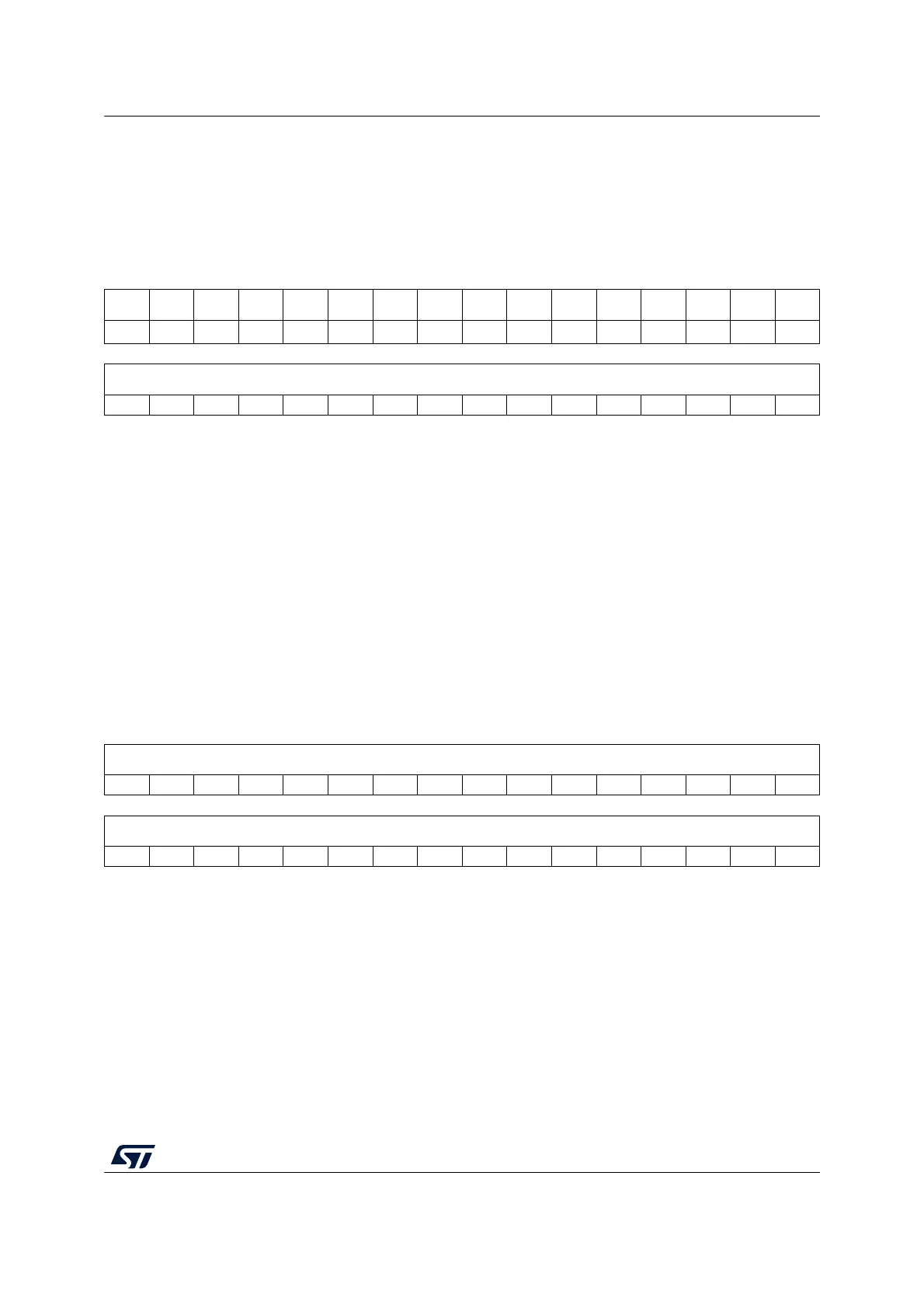
31 30 29 28 27 26 25 24 23 22 21 20 19 18 17 16
Res. Res. Res. Res. Res. Res. Res. Res. Res. Res. Res. Res. Res. Res. Res. Res.
1514131211109876543210
RXFD[15:0]
rw rw rw rw rw rw rw rw rw rw rw rw rw rw rw rw
Bits 31:16 Reserved, must be kept at reset value.
Bits 15:0 RXFD[15:0]: Rx FIFO depth
This value is in terms of 32-bit words.
Minimum value is 16
Programmed values must respect the available FIFO memory allocation and must not
exceed the power-on value.
31 30 29 28 27 26 25 24 23 22 21 20 19 18 17 16
NPTXFD/TX0FD[15:0]
rw rw rw rw rw rw rw rw rw rw rw rw rw rw rw rw
1514131211109876543210
NPTXFSA/TX0FSA[15:0]
rw rw rw rw rw rw rw rw rw rw rw rw rw rw rw rw
Bits 31:16 NPTXFD[15:0]: Non-periodic Tx FIFO depth
This value is in terms of 32-bit words.
Minimum value is 16
Programmed values must respect the available FIFO memory allocation and must not
exceed the power-on value.
Bits 15:0 NPTXFSA[15:0]: Non-periodic transmit RAM start address
This field configures the memory start address for non-periodic transmit FIFO RAM.