Inter-integrated circuit (I
2
C) interface RM0402
756/1163 RM0402 Rev 6
24.6.10 I
2
C FLTR register (I2C_FLTR)
Address offset: 0x24
Reset value: 0x0000
Bits 15:6 Reserved, must be kept at reset value
Bits 5:0 TRISE[5:0]: Maximum rise time in Fm/Sm mode (Master mode)
These bits should provide the maximum duration of the SCL feedback loop in master mode.
The purpose is to keep a stable SCL frequency whatever the SCL rising edge duration.
These bits must be programmed with the maximum SCL rise time given in the I
2
C bus
specification, incremented by 1.
For instance: in Sm mode, the maximum allowed SCL rise time is 1000 ns.
If, in the I2C_CR2 register, the value of FREQ[5:0] bits is equal to 0x08 and T
PCLK1
= 125 ns
therefore the TRISE[5:0] bits must be programmed with 09h.
(1000 ns / 125 ns = 8 + 1)
The filter value can also be added to TRISE[5:0].
If the result is not an integer, TRISE[5:0] must be programmed with the integer part, in order
to respect the t
HIGH
parameter.
Note: TRISE[5:0] must be configured only when the I2C is disabled (PE = 0).
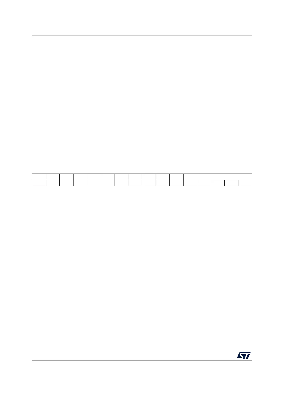
1514131211109876543210
Res. Res. Res. Res. Res. Res. Res. Res. Res. Res. Res. ANOFF DNF[3:0]
rw rw rw rw rw
Bits 15:5 Reserved, must be kept at reset value
Bit 4 ANOFF: Analog noise filter OFF
0: Analog noise filter enable
1: Analog noise filter disable
Note: ANOFF must be configured only when the I2C is disabled (PE = 0).
Bits 3:0 DNF[3:0]: Digital noise filter
These bits are used to configure the digital noise filter on SDA and SCL inputs. The digital filter
suppresses the spikes with a length of up to DNF[3:0] * TPCLK1.
0000: Digital noise filter disable
0001: Digital noise filter enabled and filtering capability up to 1* TPCLK1.
...
1111: Digital noise filter enabled and filtering capability up to 15* TPCLK1.
Note: DNF[3:0] must be configured only when the I2C is disabled (PE = 0). If the analog filter
is also enabled, the digital filter is added to the analog filter.