RM0402 Rev 6 873/1163
RM0402 Secure digital input/output interface (SDIO)
921
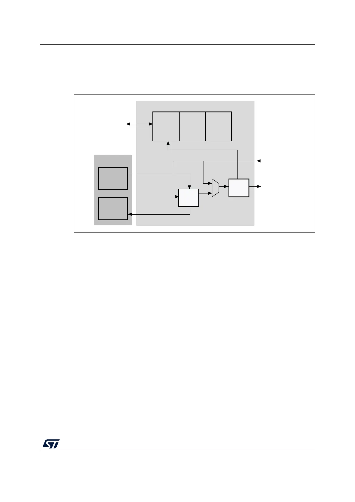
Data path
The data path subunit transfers data to and from cards. Figure 316 shows a block diagram
of the data path.
Figure 316. Data path
The card databus width can be programmed using the clock control register. If the 4-bit wide
bus mode is enabled, data is transferred at four bits per clock cycle over all four data signals
(SDIO_D[3:0]). If the 8-bit wide bus mode is enabled, data is transferred at eight bits per
clock cycle over all eight data signals (SDIO_D[7:0]). If the wide bus mode is not enabled,
only one bit per clock cycle is transferred over SDIO_D0.
Depending on the transfer direction (send or receive), the data path state machine (DPSM)
moves to the Wait_S or Wait_R state when it is enabled:
• Send: the DPSM moves to the Wait_S state. If there is data in the transmit FIFO, the
DPSM moves to the Send state, and the data path subunit starts sending data to a
card.
• Receive: the DPSM moves to the Wait_R state and waits for a start bit. When it
receives a start bit, the DPSM moves to the Receive state, and the data path subunit
starts receiving data from a card.
Data path state machine (DPSM)
The DPSM operates at SDIO_CK frequency. Data on the card bus signals is synchronous to
the rising edge of SDIO_CK. The DPSM has six states, as shown in
Figure 317: Data path
state machine (DPSM).
MSv36080V1
Data path
Data FIFO
Transmit
Status
flag
CRC
Shift
register
To control unit
SDIO_Din[7:0]
SDIO_Dout[7:0]
Receive
Control
logic
Data
timer