Serial peripheral interface/ inter-IC sound (SPI/I2S) RM0402
826/1163 RM0402 Rev 6
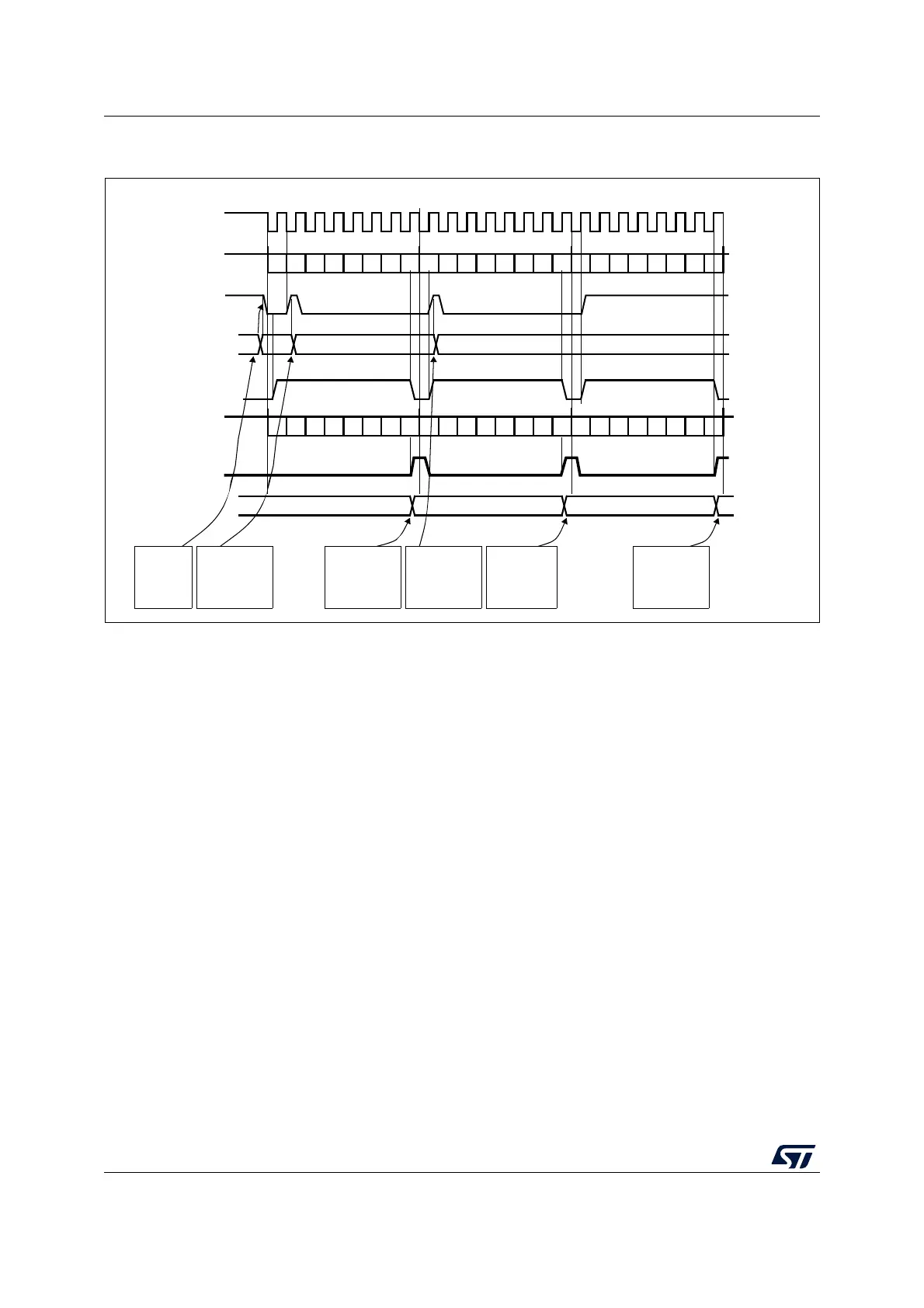
Figure 279. TXE/RXNE/BSY behavior in slave / full-duplex mode (BIDIMODE=0,
RXONLY=0) in the case of continuous transfers
26.3.10 Procedure for disabling the SPI
When SPI is disabled, it is mandatory to follow the disable procedures described in this
paragraph. It is important to do this before the system enters a low-power mode when the
peripheral clock is stopped. Ongoing transactions can be corrupted in this case. In some
modes the disable procedure is the only way to stop continuous communication running.
Master in full-duplex or transmit only mode can finish any transaction when it stops
providing data for transmission. In this case, the clock stops after the last data transaction.
Standard disable procedure is based on pulling BSY status together with TXE flag to check
if a transmission session is fully completed. This check can be done in specific cases, too,
when it is necessary to identify the end of ongoing transactions, for example:
• When NSS signal is managed by an arbitrary GPIO toggle and the master has to
provide proper end of NSS pulse for slave, or
• When transactions’ streams from DMA are completed while the last data frame or CRC
frame transaction is still ongoing in the peripheral bus.
The correct disable procedure is (except when receive-only mode is used):
1. Wait until RXNE=1 to receive the last data.
2. Wait until TXE=1 and then wait until BSY=0 before disabling the SPI.
3. Read received data.
0xF1
set by cleared by software
MISO/MOSI (in)
Tx buffer
DATA 1 = 0xA1
TXE flag
0xF2
BSY flag
0xF3
software
writes 0xF1
into SPI_DR
software waits
until TXE=1 and
writes 0xF2 into
SPI_DR
software waits
until RXNE=1
and reads 0xA1
from SPI_DR
set by hardware
cleared by software
set by hardware
cleared by software
set by hardware
SCK
DATA 2 = 0xA2
DATA 3 = 0xA3
reset by hardware
Example in Slave mode with CPOL=1, CPHA=1
RXNE flag
(write to SPI_DR)
Rx buffer
set by hardware
MISO/MOSI (out)
DATA 1 = 0xF1
DATA 2 = 0xF2
DATA 3 = 0xF3
(read from SPI_DR)
0xA1
0xA2 0xA3
software waits
until TXE=1 and
writes 0xF3 into
SPI_DR
software waits
until RXNE=1
and reads 0xA2
from SPI_ DR
software waits
until RXNE=1
and reads 0xA3
from SPI_DR
b0 b1 b2 b3 b4 b5 b6 b7 b0 b1 b2 b3 b4 b5 b6 b7 b0 b1 b2 b3 b4 b5 b6 b7
b0 b1 b2 b3 b4 b5 b6 b7 b0 b1 b2 b3 b4 b5 b6 b7 b0 b1 b2 b3 b4 b5 b6 b7
cleared by software
ai17344