Embedded Flash memory interface RM0402
74/1163 RM0402 Rev 6
3.8 Flash interface registers
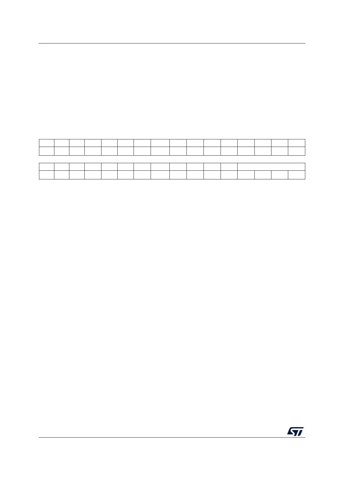
3.8.1 Flash access control register (FLASH_ACR)
The Flash access control register is used to enable/disable the acceleration features and
control the Flash memory access time according to CPU frequency.
Address offset: 0x00
Reset value: 0x0000 0000
Access: no wait state, word, half-word and byte access
31 30 29 28 27 26 25 24 23 22 21 20 19 18 17 16
Res. Res. Res. Res. Res. Res. Res. Res. Res. Res. Res. Res. Res. Res. Res. Res.
15 14 13 12 11 10 9 8 7 6 5 4 3 2 1 0
Res. Res. Res. DCRST ICRST DCEN ICEN PRFTEN Res. Res. Res. Res. LATENCY
rwwrwrw rw rwrwrwrw
Bits 31:13 Reserved, must be kept cleared.
Bit 12 DCRST: Data cache reset
0: Data cache is not reset
1: Data cache is reset
This bit can be written only when the D cache is disabled.
Bit 11 ICRST: Instruction cache reset
0: Instruction cache is not reset
1: Instruction cache is reset
This bit can be written only when the I cache is disabled.
Bit 10 DCEN: Data cache enable
0: Data cache is disabled
1: Data cache is enabled
Bit 9 ICEN: Instruction cache enable
0: Instruction cache is disabled
1: Instruction cache is enabled
Bit 8 PRFTEN: Prefetch enable
0: Prefetch is disabled
1: Prefetch is enabled
Bits 7:4 Reserved, must be kept cleared.
Bits 3:0 LATENCY: Latency
These bits represent the ratio of the CPU clock period to the Flash memory access time.
0000: Zero wait state
0001: One wait state
0010: Two wait states
-
-
-
1110: Fourteen wait states
1111: Fifteen wait states