RM0402 Rev 6 125/1163
RM0402 Reset and clock control (RCC) for STM32F412xx
166
6.3.3 RCC clock configuration register (RCC_CFGR)
Address offset: 0x08
Reset value: 0x0000 0000
Access: 0 ≤ wait state ≤ 2, word, half-word and byte access
1 or 2 wait states inserted only if the access occurs during a clock source switch.
Bits 5:0 PLLM[5:0]: Division factor for the main PLL (PLL) input clock
Set and cleared by software to divide the PLL and PLLI2S input clock before the VCO.
These bits can be written only when the PLL and PLLI2S are disabled.
Caution: The software has to set these bits correctly to ensure that the VCO input frequency
ranges from 1 to 2 MHz. It is recommended to select a frequency of 2 MHz to limit
PLL jitter.
VCO input frequency = PLL input clock frequency / PLLM with 2 ≤ PLLM ≤ 63
000000: PLLM = 0, wrong configuration
000001: PLLM = 1, wrong configuration
000010: PLLM = 2
000011: PLLM = 3
000100: PLLM = 4
...
111110: PLLM = 62
111111: PLLM = 63
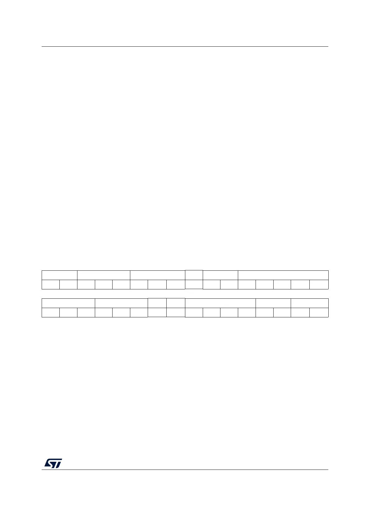
31 30 29 28 27 26 25 24 23 22 21 20 19 18 17 16
MCO2[1:0] MCO2 PRE[2:0] MCO1 PRE[2:0] Res. MCO1[1:0] RTCPRE[4:0]
rw rw rw rw rw rw rw rw rw rw rw rw rw rw
15 14 13 12 11 10 9 8 7 6 5 4 3 2 1 0
PPRE2[2:0] PPRE1[2:0] Res. Res. HPRE[3:0] SWS[1:0] SW[1:0]
rw rw rw rw rw rw rw rw rw rw r r rw rw
Bits 31:30 MCO2[1:0]: Microcontroller clock output 2
Set and cleared by software. Clock source selection may generate glitches on MCO2. It is
highly recommended to configure these bits only after reset before enabling the external
oscillators and the PLLs.
00: System clock (SYSCLK) selected
01: PLLI2S clock selected
10: HSE oscillator clock selected
11: PLL clock selected