RM0402 Rev 6 225/1163
RM0402 Direct memory access controller (DMA)
230
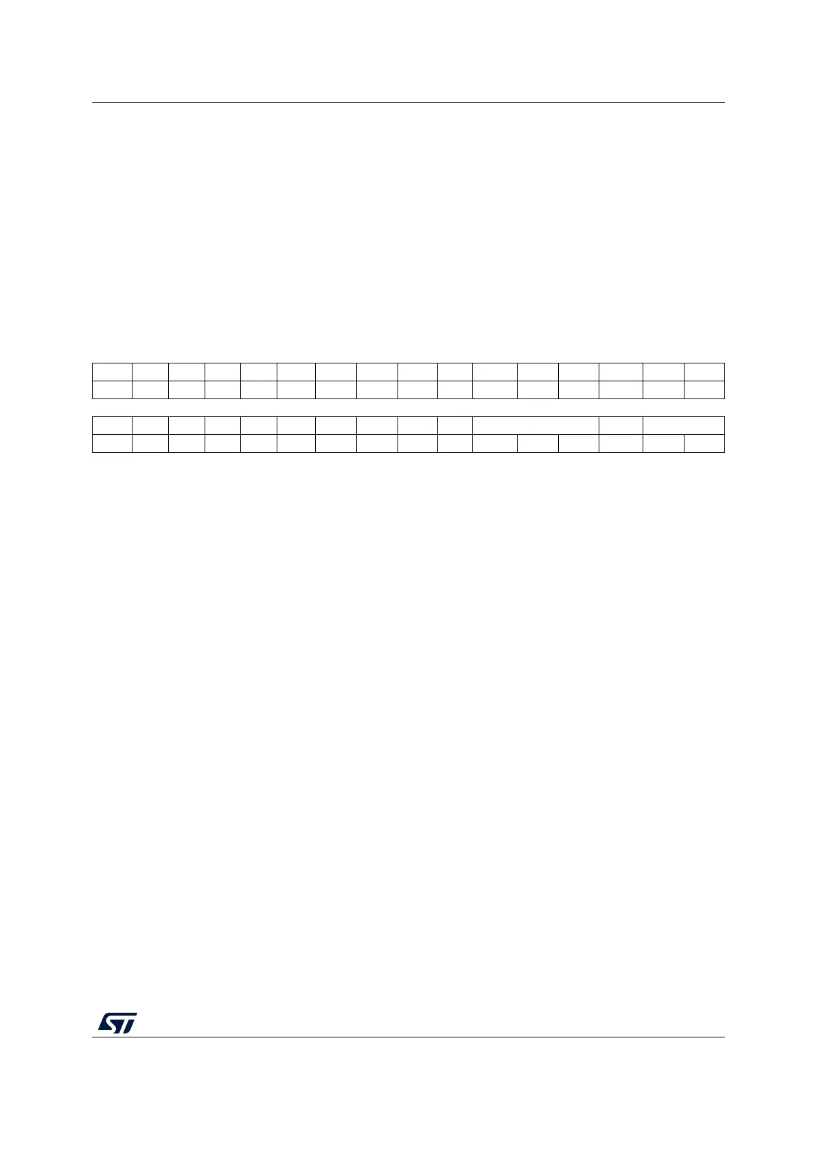
9.5.10 DMA stream x FIFO control register (DMA_SxFCR)
Address offset: 0x024 + 0x018 * x, (x = 0 to 7)
Reset value: 0x0000 0021
Bits 31:0 M1A[31:0]: memory 1 address (used in case of double-buffer mode)
Base address of memory area 1 from/to which the data is read/written.
This register is used only for the double-buffer mode.
These bits are write-protected. They can be written only if:
– the stream is disabled (EN = 0 in DMA_SxCR) or
– the stream is enabled (EN = 1 in DMA_SxCR) and bit CT = 0 in DMA_SxCR .
31 30 29 28 27 26 25 24 23 22 21 20 19 18 17 16
Res. Res. Res. Res. Res. Res. Res. Res. Res. Res. Res. Res. Res. Res. Res. Res.
15 14 13 12 11 10 9 8 7 6 5 4 3 2 1 0
Res. Res. Res. Res. Res. Res. Res. Res. FEIE Res. FS[2:0] DMDIS FTH[1:0]
rw r r r rw rw rw
Bits 31:8 Reserved, must be kept at reset value.
Bit 7 FEIE: FIFO error interrupt enable
This bit is set and cleared by software.
0: FE interrupt disabled
1: FE interrupt enabled
Bit 6 Reserved, must be kept at reset value.
Bits 5:3 FS[2:0]: FIFO status
These bits are read-only.
000: 0 < fifo_level < 1/4
001: 1/4 ≤ fifo_level < 1/2
010: 1/2 ≤ fifo_level < 3/4
011: 3/4 ≤ fifo_level < full
100: FIFO is empty
101: FIFO is full
others: no meaning
These bits are not relevant in the direct mode (DMDIS = 0).
Bit 2 DMDIS: direct mode disable
This bit is set and cleared by software. It can be set by hardware.
0: direct mode enabled
1: direct mode disabled
This bit is protected and can be written only if EN = 0.
This bit is set by hardware if the memory-to-memory mode is selected (DIR bit in
DMA_SxCR are 10) and the EN = 1 in DMA_SxCR because the direct mode is not allowed
in the memory-to-memory configuration.