Serial peripheral interface/ inter-IC sound (SPI/I2S) RM0402
854/1163 RM0402 Rev 6
26.7.2 SPI control register 2 (SPI_CR2)
Address offset: 0x04
Reset value: 0x0000
Bit 2 MSTR: Master selection
0: Slave configuration
1: Master configuration
Note: This bit should not be changed when communication is ongoing.
It is not used in I
2
S mode.
Bit1 CPOL: Clock polarity
0: CK to 0 when idle
1: CK to 1 when idle
Note: This bit should not be changed when communication is ongoing.
It is not used in I
2
S mode and SPI TI mode except the case when CRC is applied
at TI mode.
Bit 0 CPHA: Clock phase
0: The first clock transition is the first data capture edge
1: The second clock transition is the first data capture edge
Note: This bit should not be changed when communication is ongoing.
It is not used in I
2
S mode and SPI TI mode except the case when CRC is applied
at TI mode.
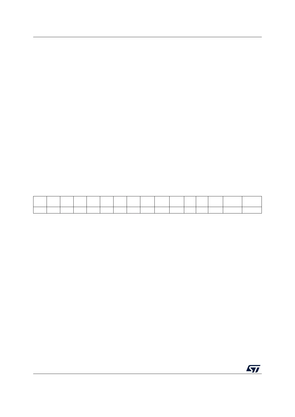
15 14 13 12 11 10 9 8 7 6 5 4 3 2 1 0
Res. Res. Res. Res. Res. Res. Res. Res. TXEIE RXNEIE ERRIE FRF Res. SSOE TXDMAEN RXDMAEN
rw rw rw rw rw rw rw
Bits 15:8 Reserved, must be kept at reset value.
Bit 7 TXEIE: Tx buffer empty interrupt enable
0: TXE interrupt masked
1: TXE interrupt not masked. Used to generate an interrupt request when the TXE flag is set.
Bit 6 RXNEIE: RX buffer not empty interrupt enable
0: RXNE interrupt masked
1: RXNE interrupt not masked. Used to generate an interrupt request when the RXNE flag is
set.
Bit 5 ERRIE: Error interrupt enable
This bit controls the generation of an interrupt when an error condition occurs (OVR,
CRCERR, MODF, FRE in SPI mode, and UDR, OVR, FRE in I
2
S mode).
0: Error interrupt is masked
1: Error interrupt is enabled
Bit 4 FRF: Frame format
0: SPI Motorola mode
1 SPI TI mode
Note: This bit is not used in I
2
S mode.
Bit 3 Reserved. Forced to 0 by hardware.