General-purpose timers (TIM9 to TIM14) RM0402
584/1163 RM0402 Rev 6
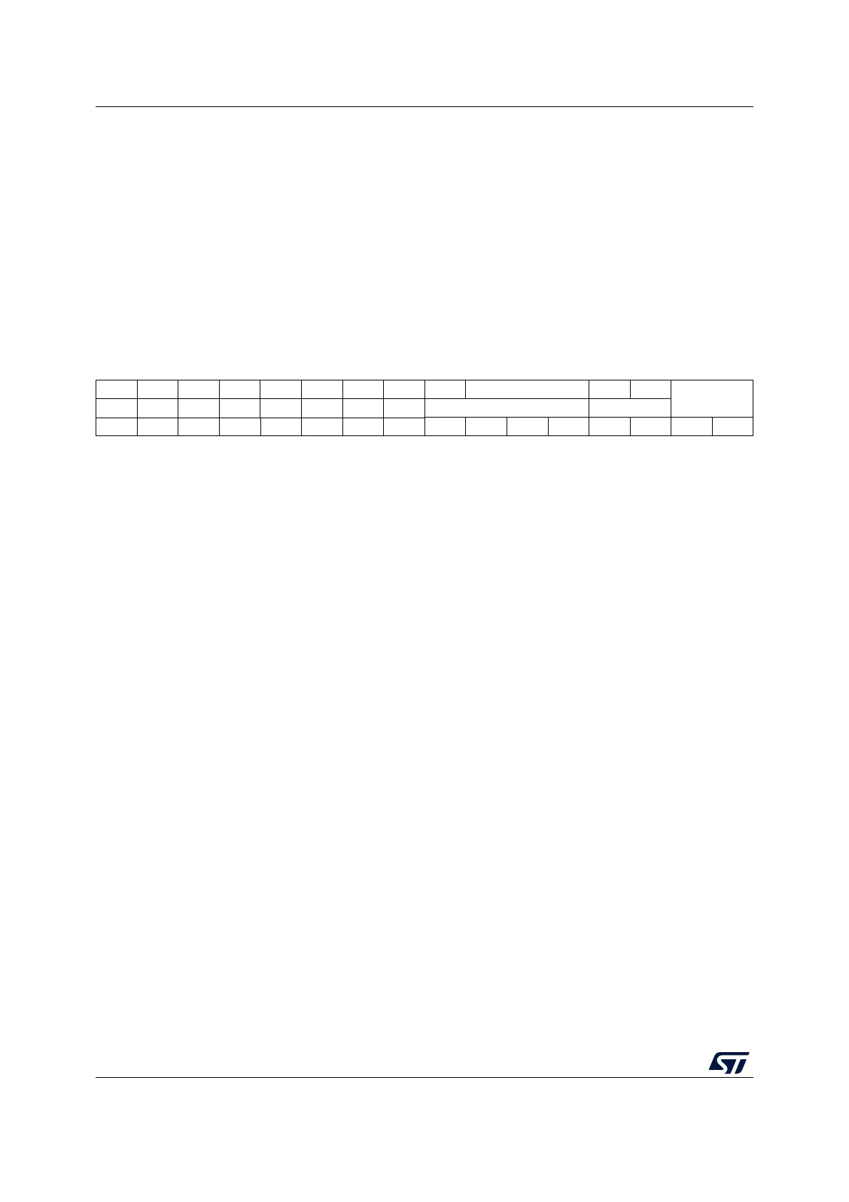
18.5.5 TIM10/11/13/14 capture/compare mode register 1
(TIMx_CCMR1)
Address offset: 0x18
Reset value: 0x0000
The channels can be used in input (capture mode) or in output (compare mode). The
direction of a channel is defined by configuring the corresponding CCxS bits. All the other
bits of this register have a different function in input and in output mode. For a given bit,
OCxx describes its function when the channel is configured in output, ICxx describes its
function when the channel is configured in input. So the user must take care that the same
bit can have a different meaning for the input stage and for the output stage.
15 14 13 12 11 10 9 8 7 6 5 4 3 2 1 0
Res. Res. Res. Res. Res. Res. Res. Res. Res. OC1M[2:0] OC1PE OC1FE
CC1S[1:0]
Res. Res. Res. Res. Res. Res. Res. Res. IC1F[3:0] IC1PSC[1:0]
rw rw rw rw rw rw rw rw