Direct memory access controller (DMA) RM0402
206/1163 RM0402 Rev 6
memory 0 to 1 (or from 1 to 0) depending on the value of CT in the DMA_SxCR register in
accordance with one of the two above conditions.
For all the other modes (except the double-buffer mode), the memory address registers are
write-protected as soon as the stream is enabled.
9.3.11 Programmable data width, packing/unpacking, endianness
The number of data items to be transferred has to be programmed into DMA_SxNDTR
(number of data items to transfer bit, NDT) before enabling the stream (except when the
flow controller is the peripheral, PFCTRL bit in DMA_SxCR is set).
When using the internal FIFO, the data widths of the source and destination data are
programmable through the PSIZE and MSIZE bits in the DMA_SxCR register (can be 8-,
16- or 32-bit).
When PSIZE and MSIZE are not equal:
• The data width of the number of data items to transfer, configured in the DMA_SxNDTR
register is equal to the width of the peripheral bus (configured by the PSIZE bits in the
DMA_SxCR register). For instance, in case of peripheral-to-memory, memory-to-
peripheral or memory-to-memory transfers and if the PSIZE[1:0] bits are configured for
half-word, the number of bytes to be transferred is equal to 2 × NDT.
• The DMA controller only copes with little-endian addressing for both source and
destination. This is described in Table 34: Packing/unpacking and endian behavior (bit
PINC = MINC = 1).
This packing/unpacking procedure may present a risk of data corruption when the operation
is interrupted before the data are completely packed/unpacked. So, to ensure data
coherence, the stream may be configured to generate burst transfers: in this case, each
group of transfers belonging to a burst are indivisible (refer to
Section 9.3.12: Single and
burst transfers).
In direct mode (DMDIS = 0 in the DMA_SxFCR register), the packing/unpacking of data is
not possible. In this case, it is not allowed to have different source and destination transfer
data widths: both are equal and defined by the PSIZE bits in the DMA_SxCR register.
MSIZE bits are not relevant.
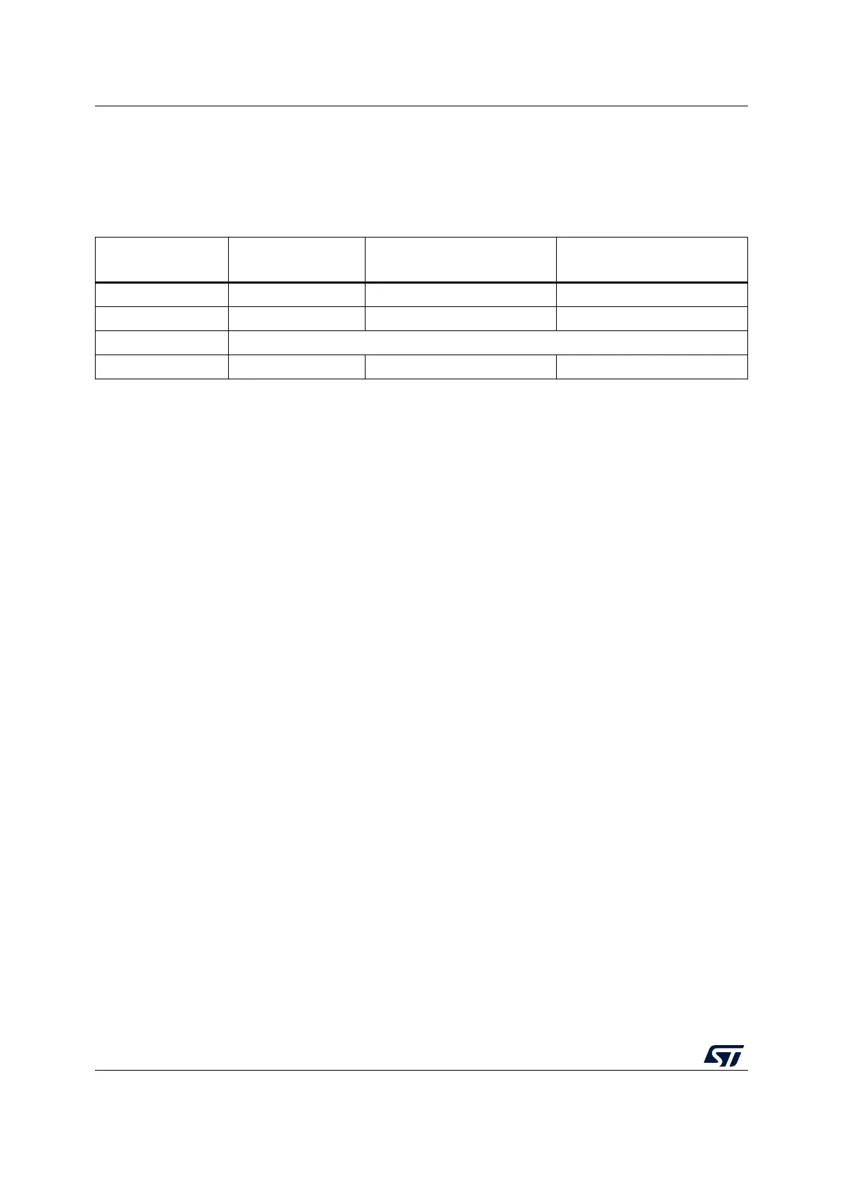
Table 33. Source and destination address registers in double-buffer mode (DBM = 1)
Bits DIR[1:0] of the
DMA_SxCR register
Direction Source address Destination address
00 Peripheral-to-memory DMA_SxPAR DMA_SxM0AR / DMA_SxM1AR
01 Memory-to-peripheral DMA_SxM0AR / DMA_SxM1AR DMA_SxPAR
10 Not allowed
(1)
11 Reserved - -
1. When the double-buffer mode is enabled, the circular mode is automatically enabled. Since the memory-to-memory mode
is not compatible with the circular mode, when the double-buffer mode is enabled, it is not allowed to configure the
memory-to-memory mode.