Embedded Flash memory interface RM0402
60/1163 RM0402 Rev 6
3.4 Read interface
3.4.1 Relation between CPU clock frequency and Flash memory read time
To correctly read data from Flash memory, the number of wait states (LATENCY) must be
correctly programmed in the Flash access control register (FLASH_ACR) according to the
frequency of the CPU clock (HCLK) and the supply voltage of the device.
The prefetch buffer must be disabled when the supply voltage is below 2.1 V. The
correspondence between wait states and CPU clock frequency is given in
Table 8:
• When VOS[1:0] = 0x01, the maximum value of f
HCLK
= 64 MHz.
• When VOS[1:0] = 0x10, the maximum value of f
HCLK
= 84 MHz.
• When VOS[1:0] = 0x11, the maximum value of f
HCLK
= 100 MHz.
After reset, the CPU clock frequency is 16 MHz and 0 wait state (WS) is configured in the
FLASH_ACR register.
It is highly recommended to use the following software sequences to tune the number of
wait states needed to access the Flash memory with the CPU frequency.
Increasing the CPU frequency
1. Program the new number of wait states to the LATENCY bits in the FLASH_ACR
register
2. Check that the new number of wait states is taken into account to access the Flash
memory by reading the FLASH_ACR register
3. Modify the CPU clock source by writing the SW bits in the RCC_CFGR register
4. If needed, modify the CPU clock prescaler by writing the HPRE bits in RCC_CFGR
5. Check that the new CPU clock source or/and the new CPU clock prescaler value is/are
taken into account by reading the clock source status (SWS bits) or/and the AHB
prescaler value (HPRE bits), respectively, in the RCC_CFGR register.
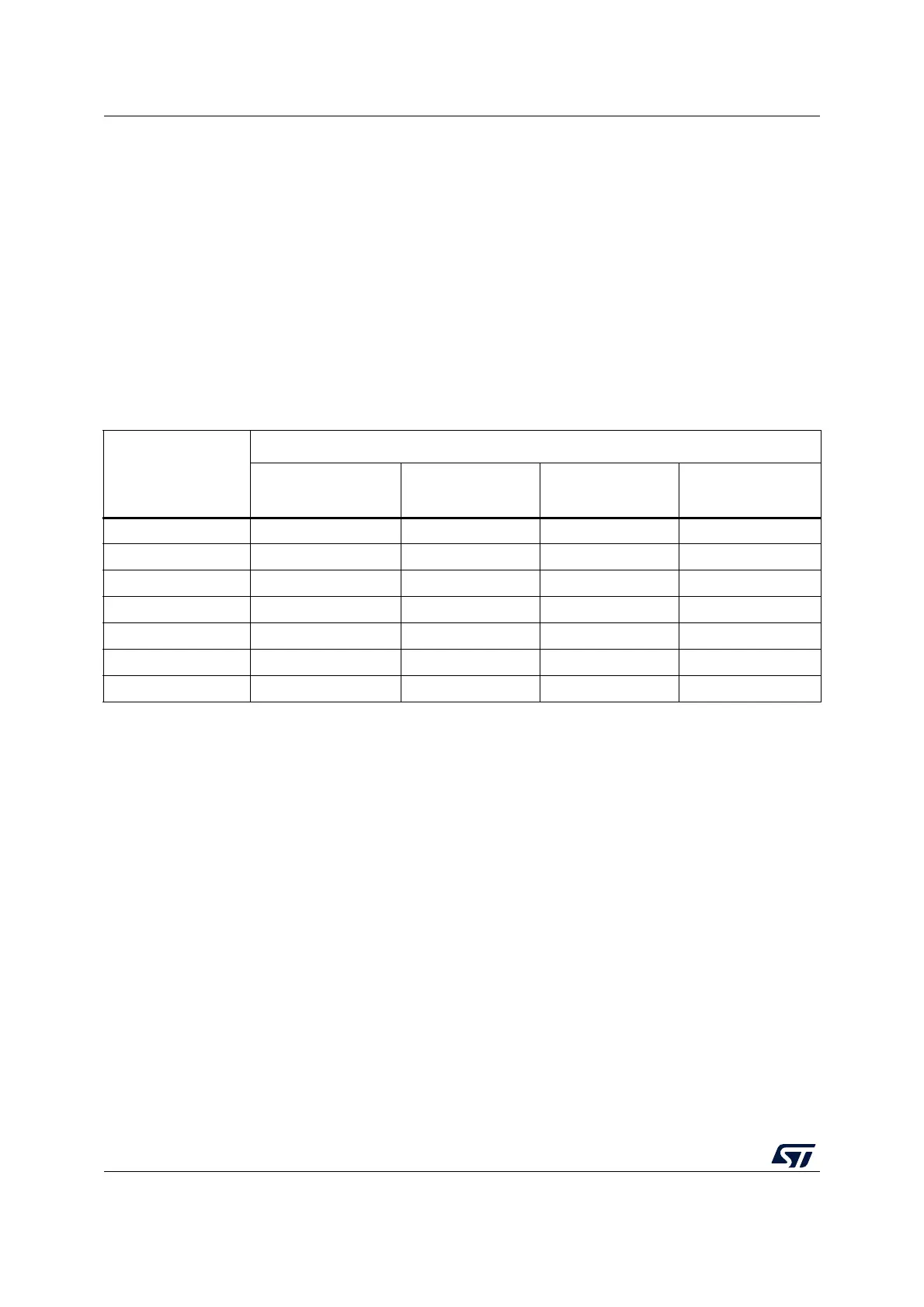
Table 6. Number of wait states according to CPU clock (HCLK) frequency
Wait states (WS)
(LATENCY)
HCLK (MHz)
Voltage range
2.7 V - 3.6 V
Voltage range
2.4 V - 2.7 V
Voltage range
2.1 V - 2.4 V
Voltage range
1.7 V - 2.1 V
0 WS (1 CPU cycle) 0 < HCLK ≤ 30 0 < HCLK ≤ 24 0 < HCLK ≤ 18 0 < HCLK ≤ 16
1 WS (2 CPU cycles) 30 < HCLK ≤ 64 24 < HCLK ≤ 48 18 < HCLK ≤ 36 16 <HCLK ≤ 32
2 WS (3 CPU cycles) 64 < HCLK ≤ 90 48 < HCLK ≤ 72 36 < HCLK ≤ 54 32 < HCLK ≤ 48
3 WS (4 CPU cycles) 90 < HCLK ≤ 100 72 < HCLK ≤ 96 54 < HCLK ≤ 72 48 < HCLK ≤ 64
4 WS (5 CPU cycles) - 96 < HCLK ≤ 100 72 < HCLK ≤ 90 64 < HCLK ≤ 80
5 WS (6 CPU cycles) - - 90 < HCLK ≤ 100 80 < HCLK ≤ 96
6 WS (7 CPU cycles) - - - 96 < HCLK ≤ 100