RM0402 Rev 6 315/1163
RM0402 Quad-SPI interface (QUADSPI)
316
12.5.12 QUADSPI polling interval register (QUADSPI_PIR)
Address offset: 0x002C
Reset value: 0x0000 0000
12.5.13 QUADSPI low-power timeout register (QUADSPI_LPTR)
Address offset: 0x0030
Reset value: 0x0000 0000
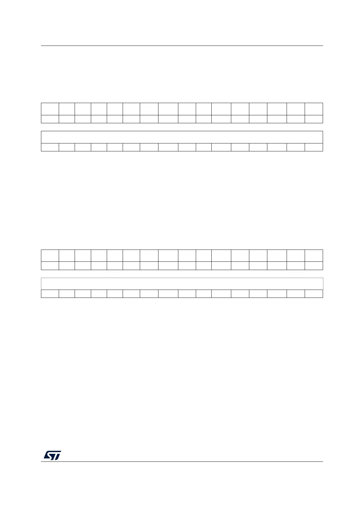
31 30 29 28 27 26 25 24 23 22 21 20 19 18 17 16
Res. Res. Res. Res. Res. Res. Res. Res. Res. Res. Res. Res. Res. Res. Res. Res.
15 14 13 12 11 10 9 8 7 6 5 4 3 2 1 0
INTERVAL[15:0]
rw rw rw rw rw rw rw rw rw rw rw rw rw rw rw rw
Bits 31:16 Reserved, must be kept at reset value.
Bits 15:0 INTERVAL[15:0]: Polling interval
Number of CLK cycles between to read during automatic polling phases.
This field can be written only when BUSY = 0.
31 30 29 28 27 26 25 24 23 22 21 20 19 18 17 16
Res. Res. Res. Res. Res. Res. Res. Res. Res. Res. Res. Res. Res. Res. Res. Res.
15 14 13 12 11 10 9 8 7 6 5 4 3 2 1 0
TIMEOUT[15:0]
rw rw rw rw rw rw rw rw rw rw rw rw rw rw rw rw
Bits 31:16 Reserved, must be kept at reset value.
Bits 15:0 TIMEOUT[15:0]: Timeout period
After each access in memory-mapped mode, the QUADSPI prefetches the subsequent
bytes and holds these bytes in the FIFO. This field indicates how many CLK cycles the
QUADSPI waits after the FIFO becomes full until it raises nCS, putting the Flash
memory in a lower-consumption state.
This field can be written only when BUSY = 0.