RM0402 Rev 6 53/1163
RM0402
57
2.3 Embedded SRAM
STM32F412xx devices feature 256 Kbytes of system SRAM.
The embedded SRAM can be accessed as bytes, half-words (16 bits) or full words (32 bits).
Read and write operations are performed at CPU speed with 0 wait state.
The CPU can access the embedded SRAM1, through the System Bus or through the I-
Code/D-Code buses when boot from SRAM is selected or when physical remap is selected
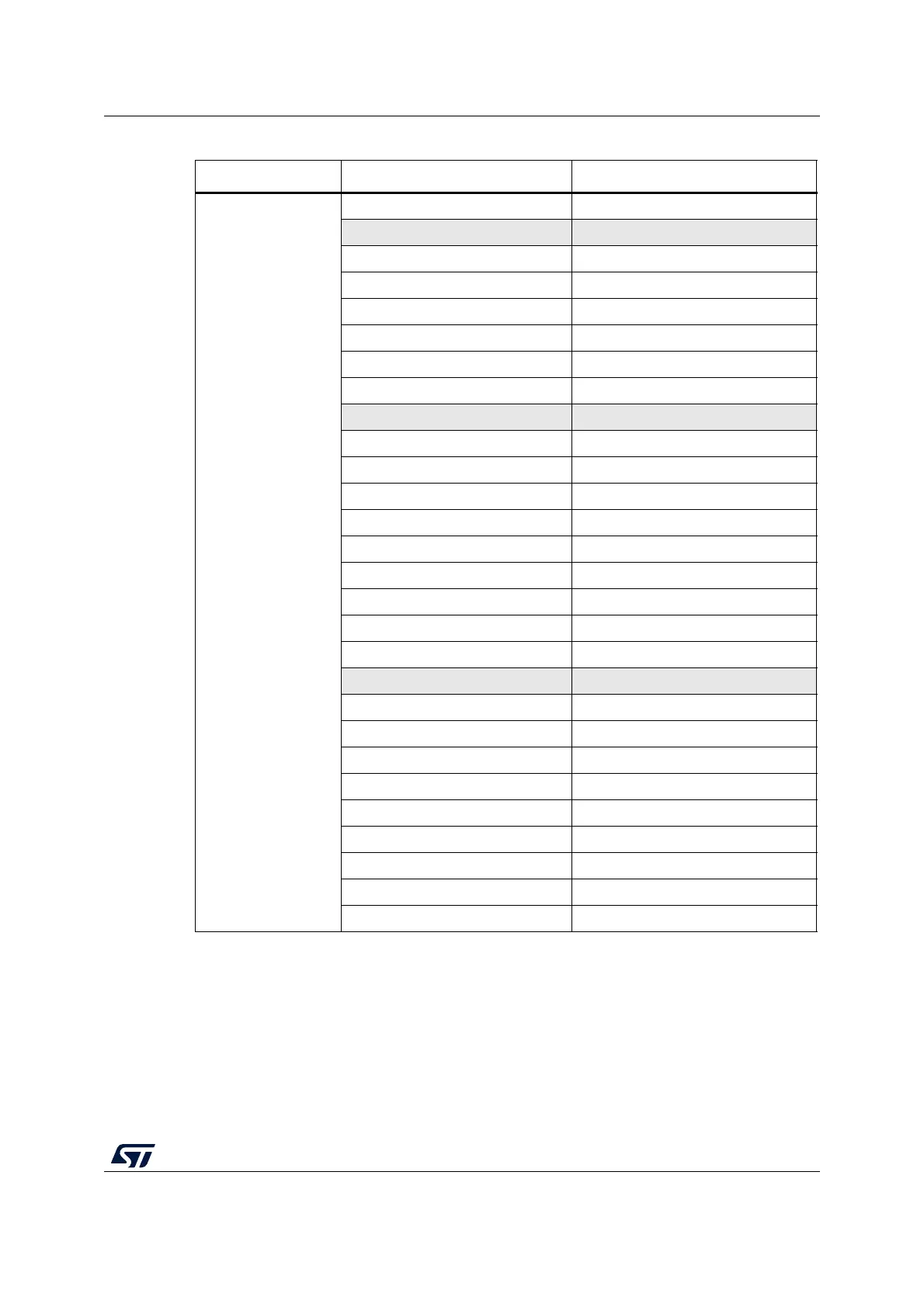
APB1
0x4000 7000 - 0x4000 73FF PWR
0x4000 6C00 - 0x4000 6FFF Reserved
0x4000 6800 - 0x4000 6BFF CAN2
0x4000 6400 - 0x4000 67FF CAN1
0x4000 6000 - 0x4000 63FF I2CFMP1
0x4000 5C00 - 0x4000 5FFF I2C3
0x4000 5800 - 0x4000 5BFF I2C2
0x4000 5400 - 0x4000 57FF I2C1
0x4000 4C00 - 0x4000 53FF Reserved
0x4000 4800 - 0x4000 4BFF USART3
0x4000 4400 - 0x4000 47FF USART2
0x4000 4000 - 0x4000 3FFF I2S3ext
0x4000 3C00 - 0x4000 3FFF SPI3 / I2S3
0x4000 3800 - 0x4000 3BFF SPI2 / I2S2
0x4000 3400 - 0x4000 37FF I2S2ext
0x4000 3000 - 0x4000 33FF IWDG
0x4000 2C00 - 0x4000 2FFF WWDG
0x4000 2800 - 0x4000 2BFF RTC & BKP Registers
0x4000 2400 - 0x4000 27FF Reserved
0x4000 2000 - 0x4000 23FF TIM14
0x4000 1C00 - 0x4000 1FFF TIM13
0x4000 1800 - 0x4000 1BFF TIM12
0x4000 1400 - 0x4000 17FF TIM7
0x4000 1000 - 0x4000 13FF TIM6
0x4000 0C00 - 0x4000 0FFF TIM5
0x4000 0800 - 0x4000 0BFF TIM4
0x4000 0400 - 0x4000 07FF TIM3
0x4000 0000 - 0x4000 03FF TIM2
Table 1. Register boundary addresses (continued)
Bus Boundary address Peripheral