Secure digital input/output interface (SDIO) RM0402
900/1163 RM0402 Rev 6
27.5.1 R1 (normal response command)
Code length = 48 bits. The 45:40 bits indicate the index of the command to be responded to,
this value being interpreted as a binary-coded number (between 0 and 63). The status of the
card is coded in 32 bits.
27.5.2 R1b
It is identical to R1 with an optional busy signal transmitted on the data line. The card may
become busy after receiving these commands based on its state prior to the command
reception.
27.5.3 R2 (CID, CSD register)
Code length = 136 bits. The contents of the CID register are sent as a response to the
CMD2 and CMD10 commands. The contents of the CSD register are sent as a response to
CMD9. Only the bits [127...1] of the CID and CSD are transferred, the reserved bit [0] of
these registers is replaced by the end bit of the response. The card indicates that an erase
is in progress by holding SDIO_D0 low. The actual erase time may be quite long, and the
host may issue CMD7 to deselect the card.
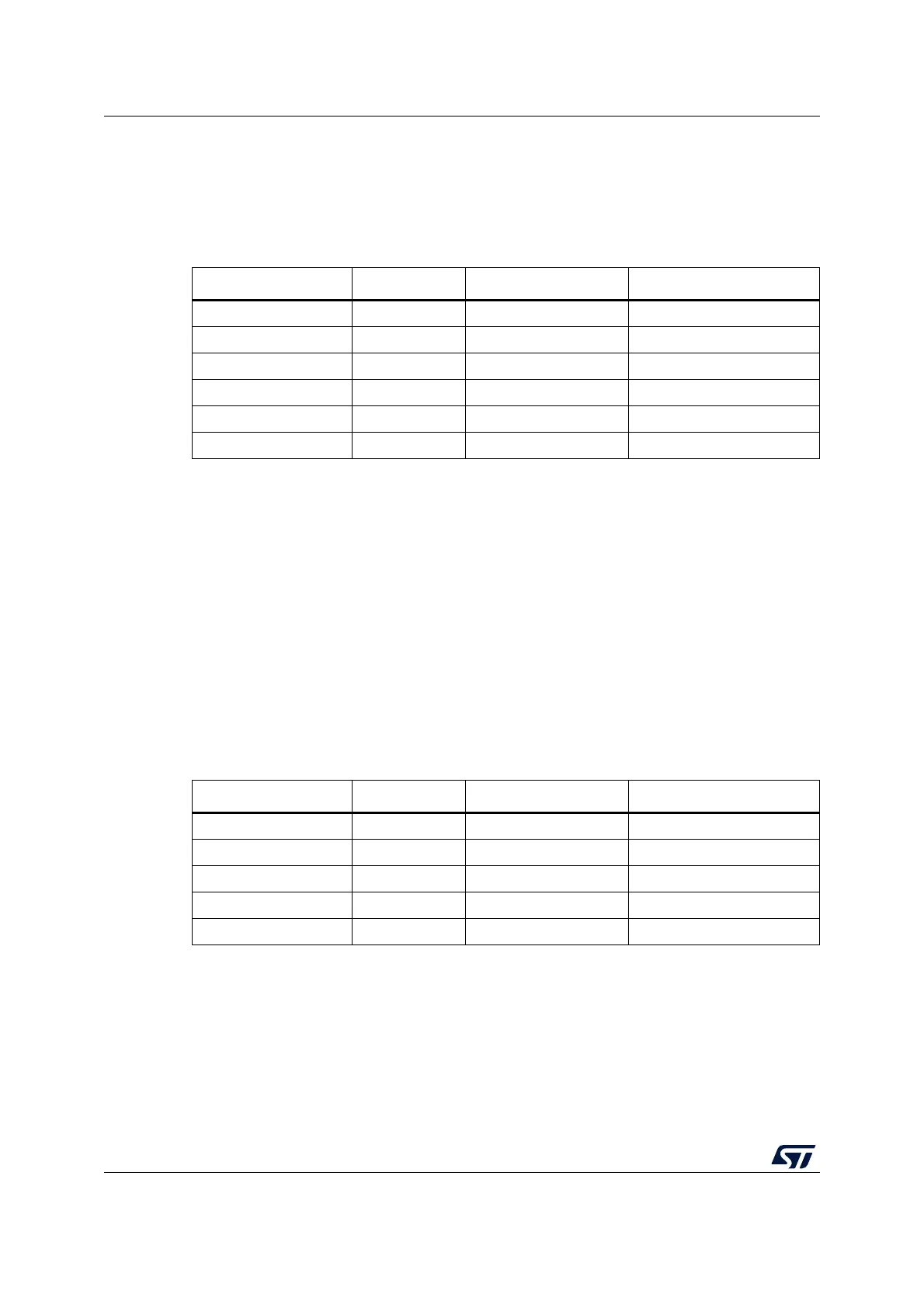
Table 184. R1 response
Bit position Width (bits Value Description
47 1 0 Start bit
46 1 0 Transmission bit
[45:40] 6 X Command index
[39:8] 32 X Card status
[7:1] 7 X CRC7
011 End bit
Table 185. R2 response
Bit position Width (bits Value Description
135 1 0 Start bit
134 1 0 Transmission bit
[133:128] 6 ‘111111’ Command index
[127:1] 127 X Card status
011 End bit