RM0402 Rev 6 755/1163
RM0402 Inter-integrated circuit (I
2
C) interface
757
24.6.9 I
2
C TRISE register (I2C_TRISE)
Address offset: 0x20
Reset value: 0x0002
Bit 14 DUTY: Fm mode duty cycle
0: Fm mode t
low
/t
high
= 2
1: Fm mode t
low
/t
high
= 16/9 (see CCR)
Note: When the PCLK frequency is a multiple of 10 MHz, the DUTY bit must be set in order to
reach the 400 kHz maximum I2C frequency.
Bits 13:12 Reserved, must be kept at reset value
Bits 11:0 CCR[11:0]: Clock control register in Fm/Sm mode (Master mode)
Controls the SCL clock in master mode.
Sm mode or SMBus
:
T
high
= CCR * T
PCLK1
T
low
= CCR * T
PCLK1
Fm mode:
If DUTY = 0:
T
high
= CCR * T
PCLK1
T
low
= 2 * CCR * T
PCLK1
If DUTY = 1:
T
high
= 9 * CCR * T
PCLK1
T
low
= 16 * CCR * T
PCLK1
For instance: in Sm mode, to generate a 100 kHz SCL frequency:
If FREQ = 08, T
PCLK1
= 125 ns so CCR must be programmed with 0x28
(0x28 <=> 40d x 125 ns = 5000 ns.)
Note: The minimum allowed value is 0x04, except in FAST DUTY mode where the minimum
allowed value is 0x01
t
high
= t
r(SCL)
+ t
w(SCLH)
. See device datasheet for the definitions of parameters.
t
low
= t
f(SCL)
+ t
w(SCLL)
. See device datasheet for the definitions of parameters.
I2C communication speed, fSCL ~ 1/(thigh + tlow). The real frequency may differ due to
the analog noise filter input delay.
The CCR register must be configured only when the I
2
C is disabled (PE = 0).
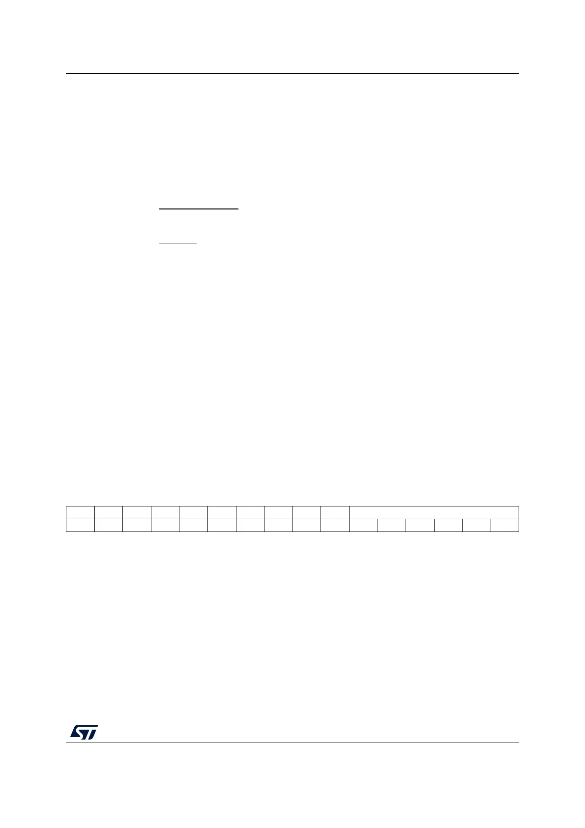
15 14 13 12 11 10 9 8 7 6 5 4 3 2 1 0
Res. Res. Res. Res. Res. Res. Res. Res. Res. Res. TRISE[5:0]
rw rw rw rw rw rw