MPC5604B/C Microcontroller Reference Manual, Rev. 8
718 Freescale Semiconductor
For additional information on the address-based read access timing for emulation of other memory types,
see Section 27.8.11, Wait-state emulation”.
Next, consider the memory map associated with the control and configuration registers.
Regardless of the number of populated banks or the number of flash memory arrays included in a given
bank, the configuration of the platform flash memory controller is wholly specified by the platform flash
memory controller registers associated with code flash memory array 0. The code array0 register settings
define the operating behavior of both flash memory banks; it is recommended that the platform flash
memory controller registers for all physically-present arrays be set to the code flash memory array0 values.
NOTE
To perform program and erase operations, the control registers in the actual
referenced flash memory array must be programmed, but the configuration
of the platform flash memory controller module is defined by the platform
flash controller registers of code array0.
The 32-bit memory map for the platform flash memory controller control registers is shown in
Table 27-57. The base address of the controller is 0xC3F8_8000.
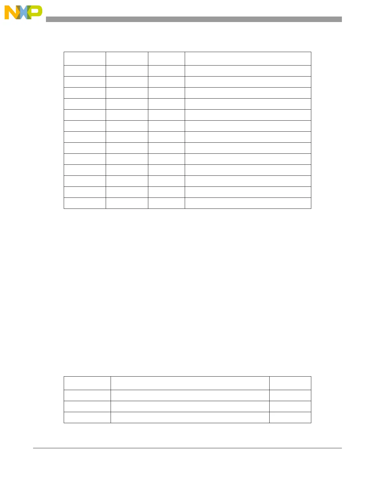
Table 27-56. Flash memory-related regions in the system memory map
Start address End address Size [KB] Region
0x0000_0000 0x0007_FFFF 512 Code flash memory array 0
0x0008_0000 0x001F_FFFF 1536 Reserved
0x0020_0000 0x0027_FFFF 16 Code flash memory array 0: shadow sector
0x0028_0000 0x002F_FFFF 1536 Reserved
0x0040_0000 0x0040_3FFF 16 Code flash memory array 0: test sector
0x0040_4000 0x007F_FFFF 4078 Reserved
0x0080_0000 0x0080_FFFF 64 Data flash memory array 0
0x0081_0000 0x00BF_FFFF 4032 Reserved
0x00C0_0000 0x00C7_FFFF 16 Data flash memory array 0: test sector
0x00C8_0000 0x00FF_FFFF 3584 Reserved
0x0100_0000 0x1FFF_FFFF 507904 Emulation mapping
0xC3F8_8000 0xC3F8_BFFF 16 Code flash memory array 0 configuration
0xC3F8_C000 0xC3F8_FFFF 16 Data flash memory array 0 configuration
Table 27-57. Platform flash memory controller 32-bit memory map
Address offset Register Location
0x1C Platform Flash Configuration Register 0 (PFCR0) on page 719
0x20 Platform Flash Configuration Register 1 (PFCR1) on page 722
0x24 Platform Flash Access Protection Register (PFAPR) on page 724
 Loading...