Flexible static memory controller (FSMC) RM0402
282/1163 RM0402 Rev 6
one to configure read accesses (this register) and one to configure write accesses
(FSMC_BWTRx registers).
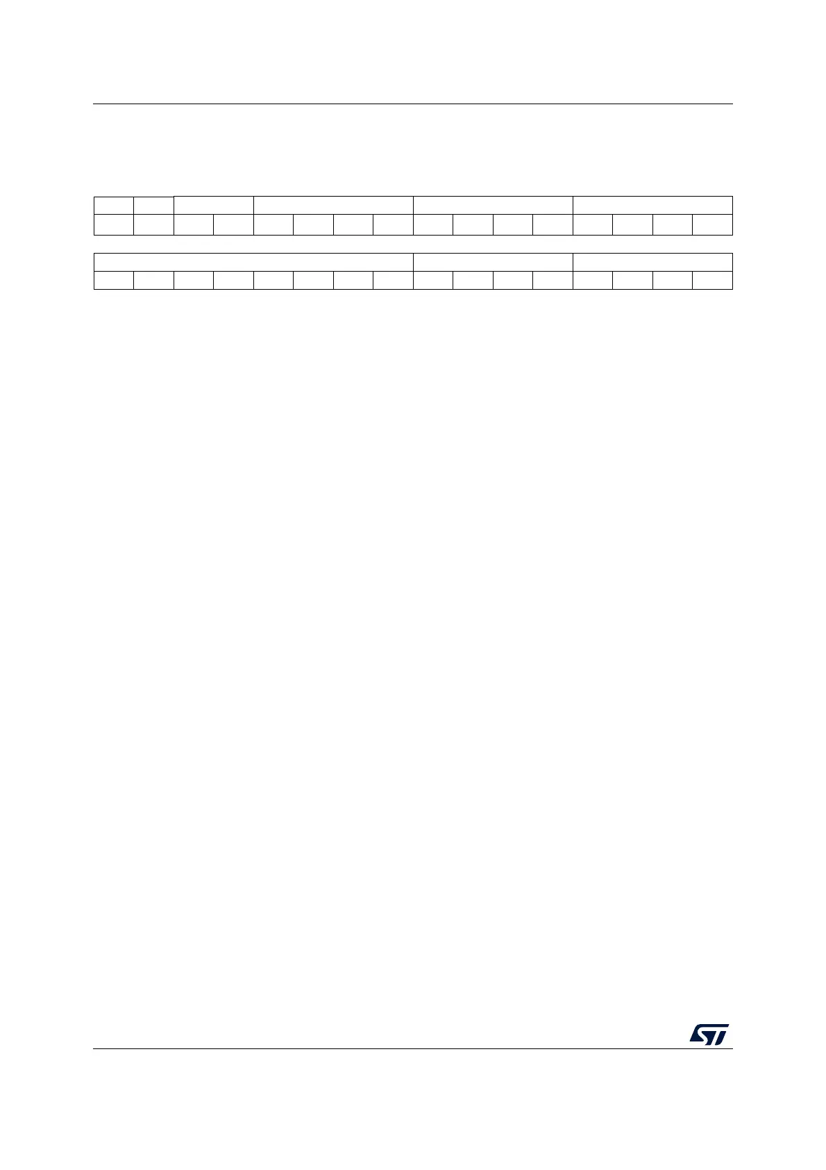
31 30 29 28 27 26 25 24 23 22 21 20 19 18 17 16
Res. Res. ACCMOD[1:0] DATLAT[3:0] CLKDIV[3:0] BUSTURN[3:0]
rw rw rw rw rw rw rw rw rw rw rw rw rw rw
1514131211109876543210
DATAST[7:0] ADDHLD[3:0] ADDSET[3:0]
rw rw rw rw rw rw rw rw rw rw rw rw rw rw rw rw
Bits 31:30 Reserved, must be kept at reset value.
Bits 29:28 ACCMOD[1:0]: Access mode
Specifies the asynchronous access modes as shown in the timing diagrams. These bits are
taken into account only when the EXTMOD bit in the FSMC_BCRx register is 1.
00: Access mode A
01: Access mode B
10: Access mode C
11: Access mode D
Bits 27:24 DATLAT[3:0]: (see note below bit descriptions): Data latency for synchronous memory
For synchronous access with read/write Burst mode enabled (BURSTEN / CBURSTRW bits
set), defines the number of memory clock cycles (+2) to issue to the memory before
reading/writing the first data:
This timing parameter is not expressed in HCLK periods, but in FSMC_CLK periods.
For asynchronous access, this value is don't care.
0000: Data latency of 2 CLK clock cycles for first burst access
1111: Data latency of 17 CLK clock cycles for first burst access (default value after reset)
Bits 23:20 CLKDIV[3:0]: Clock divide ratio (for FSMC_CLK signal)
Defines the period of FSMC_CLK clock output signal, expressed in number of HCLK cycles:
0000: FSMC_CLK period= 1x HCLK period
0001: FSMC_CLK period = 2 × HCLK periods
0010: FSMC_CLK period = 3 × HCLK periods
1111: FSMC_CLK period = 16 × HCLK periods (default value after reset)
In asynchronous NOR Flash, SRAM or PSRAM accesses, this value is don’t care.
Note: Refer to Section 11.6.5: Synchronous transactions for FSMC_CLK divider ratio formula)