MPC5604B/C Microcontroller Reference Manual, Rev. 8
536 Freescale Semiconductor
Addresses of Unified Channel registers are specified as offsets from the channel’s base address; otherwise
the eMIOS base address is used as reference.
Table 24-10 describes the Unified Channel memory map.
24.4.3.2 Register description
All control registers are 32 bits wide. Data registers and counter registers are 16 bits wide.
24.4.3.2.1 eMIOS Module Configuration Register (EMIOSMCR)
The EMIOSMCR contains global control bits for the eMIOS block.
Table 24-10. Unified Channel memory map
UC[n] base address Description Location
0x00 eMIOS UC A Register (EMIOSA[n]) on page 539
0x04 eMIOS UC B Register (EMIOSB[n]) on page 540
0x08 eMIOS UC Counter Register (EMIOSCNT[n]) on page 541
0x0C eMIOS UC Control Register (EMIOSC[n]) on page 541
0x10 eMIOS UC Status Register (EMIOSS[n]) on page 545
0x14 eMIOS UC Alternate A Register (EMIOSALTA[n]) on page 546
0x18–0x1F Reserved —
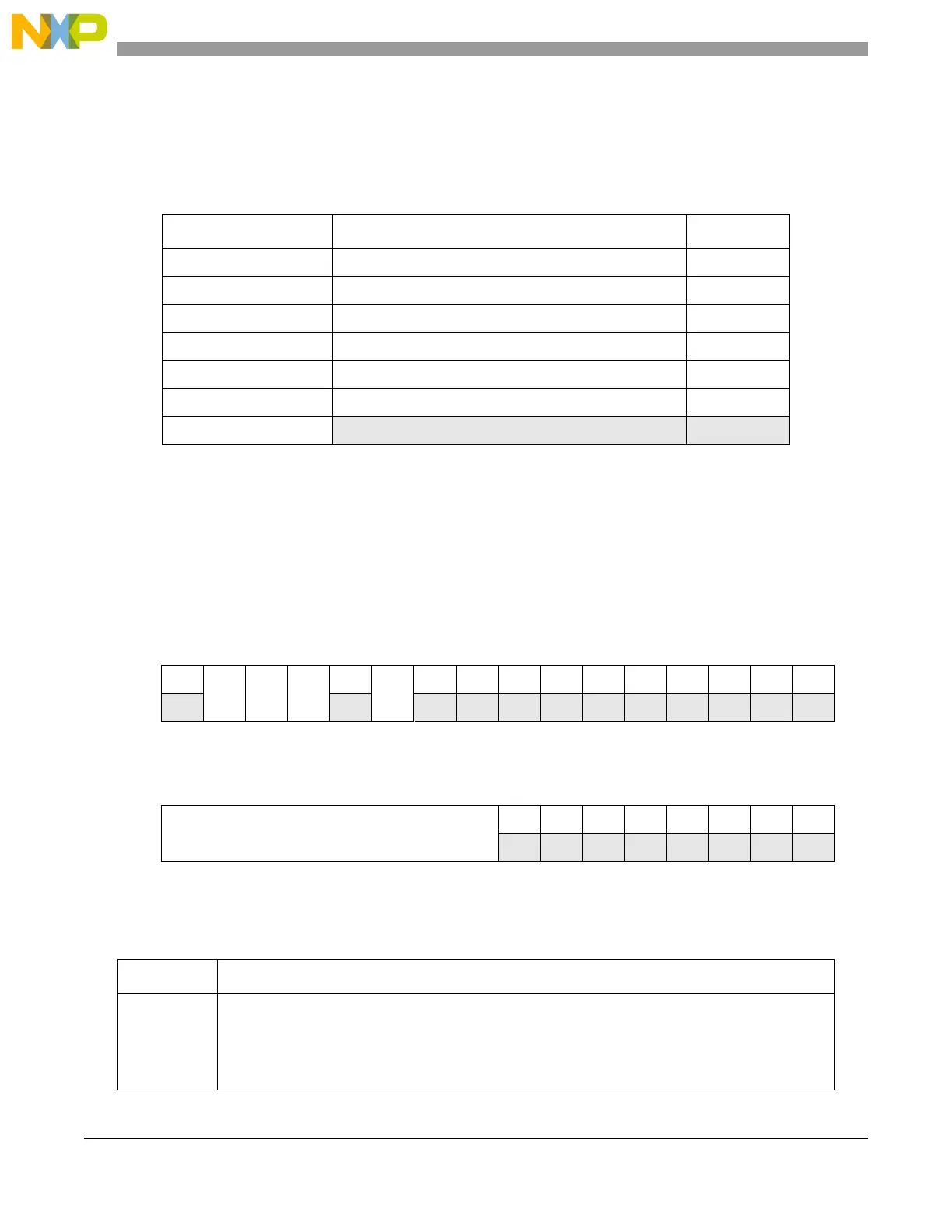
Address: eMIOS base address +0x00
0123456789101112131415
R0
MDIS FRZ
GTBE
0
GPREN
0000000000
W
Reset0000000000000000
16 17 18 19 20 21 22 23 24 25 26 27 28 29 30 31
R
GPRE
00000000
W
Reset0000000000000000
Figure 24-8. eMIOS Module Configuration Register (EMIOSMCR)
Table 24-11. EMIOSMCR field descriptions
Field Description
MDIS Module Disable
Puts the eMIOS in low power mode. The MDIS bit is used to stop the clock of the block, except the
access to registers EMIOSMCR, EMIOSOUDIS and EMIOSUCDIS.
1 = Enter low power mode
0 = Clock is running