System Debug
11-10 Copyright © 2005-2008 ARM Limited. All rights reserved. ARM DDI 0337G
Non-Confidential
Unrestricted Access
• COMP is the matching comparator. See Table 11-3.
• HADDR[1:0] is the two Least Significant Bits (LSBs) of the original address.
HADDR[1:0] is always 2’b00 for instruction fetches.
The register address, access type, and Reset state are:
Address
0xE0002004
Access Read/write
Reset state This register is not reset
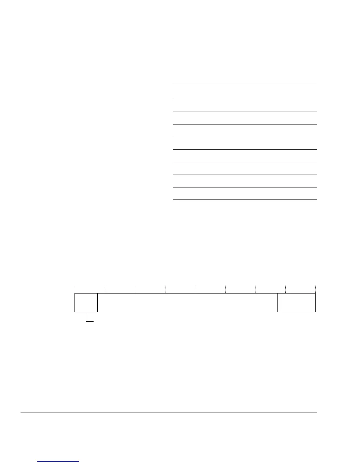
Figure 11-3 shows the bit assignments of the Flash Patch Remap Register.
Figure 11-3 Flash Patch Remap Register bit assignments
Table 11-3 COMP mapping
COMP[2:0] Comparator Description
000 FP_COMP0 Instruction comparator
001 FP_COMP1 Instruction comparator
010 FP_COMP2 Instruction comparator
011 FP_COMP3 Instruction comparator
100 FP_COMP4 Instruction comparator
101 FP_COMP5 Instruction comparator
110 FP_COMP6 Literal comparator
111 FP_COMP7 Literal comparator
31 0
Reserved
4529 28
REMAP
Reserved