Memory Protection Unit
ARM DDI 0337G Copyright © 2005-2008 ARM Limited. All rights reserved. 9-13
Unrestricted Access Non-Confidential
9.3 MPU access permissions
This section describes the MPU access permissions. The access permission bits, TEX,
C, B, AP, and XN, of the Region Access Control Register (see MPU Region Attribute
and Size Register on page 9-8) control access to the corresponding memory region. If
an access is made to an area of memory without the required permissions, then a
permission fault is raised.
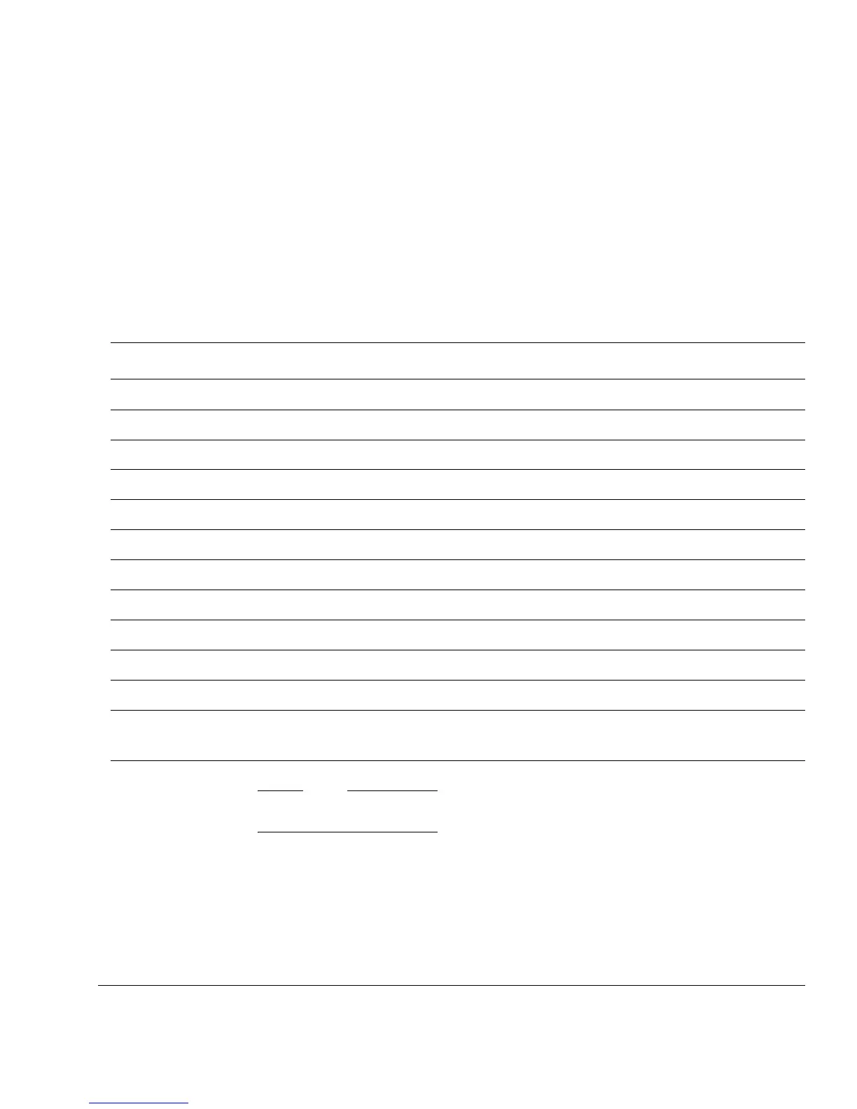
Table 9-8 describes the TEX, C, and B encoding.
Note
In Table 9-8, S is the S bit [2] from the MPU Region Attributes and Size Register.
Table 9-8 TEX, C, B encoding
TEX C B Description Memory type Region shareability
b000 0 0 Strongly ordered. Strongly ordered Shareable
b000 0 1 Shared device. Device Shareable
b000 1 0 Outer and inner write-through. No write allocate. Normal S
b000 1 1 Outer and inner write-back. No write allocate. Normal S
b001 0 0 Outer and inner noncacheable. Normal S
b001 0 1 Reserved. Reserved Reserved
b001 1 0 Implementation-defined.
b001 1 1 Outer and inner write-back. Write and read allocate. Normal S
b010 0 0 Nonshared device. Device Not shareable
b010 0 1 Reserved. Reserved Reserved
b010 1 X Reserved. Reserved Reserved
b1BB A A Cached memory BB = outer policy.
AA = inner policy.
Normal S